


制造商零件编号 DKS-PCB-RULER-12INCH
PCB LAYOUT REFERENCE RULER 12"
DigiKey Standard
It’s never been easier to bring your electronics project from a breadboard to a custom printed circuit board (PCB).
This is part of my series here on DigiKey, which has over twenty installments filled with answers to all the questions beginners ask. If you’re totally new to electronics, watch the first few episodes to get the background info needed to understand this intermediate-level topic.


Open Hardware Summit 2024 badge
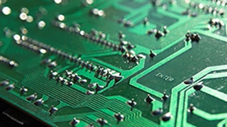
Printed circuit boards, or PCBs, are in almost every electronic product you can find today. The colorful little boards host tiny cities of components and conductive traces connecting them, like roads for the electrons to follow. They’re made up of layers.
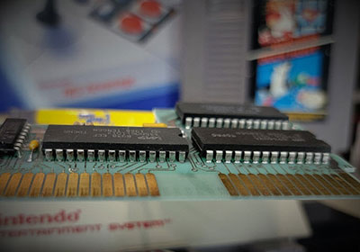
Rigid boards are made from fiberglass and have a copper layer on one or both sides. More advanced boards even have multiple layers of copper in the middle of the sandwich.
 Flex PCB inside the Reebok Checklight product
Flexible PCBs are made of polyimide and can be considerably thinner than even the thinnest fiberglass board.
 Images: Stephen Hawes
This big plane of conductive metal is then shaped into the circuit design of choice through a photochemical process that removes the material everywhere the circuit isn’t. The material applied is called a resist layer because it resists the etchant from getting to the copper below.

Then a few more layers are applied on top. One is the solder mask, which covers up all the traces but leaves the solder pads exposed.
 Orange solder mask with a white silkscreen layer
Then on top of that is the silkscreen layer, which is for graphics and labeling things. Yes, the same type of silkscreen used for t-shirts.
 King Credie PCB factory / Image: David Cranor
This is the way commercial circuit boards are manufactured. It’s a specialized process that isn’t easily spun up or shut down, so that’s why you usually send your designs to a board house instead of doing it yourself. They’re making circuit boards all day every day and require large batches of boards to process at once.
For a more technical introduction to PCBs, check out this episode of the Another Teaching Moment series here on DigiKey– it goes into more detail on things like plated through holes.

Besides going to the board house directly, there are a few options for getting your small batch of boards made, one of which is DigiKey’s DK Red service. Your order for a small number of boards is combined with other customers on a large panel, which is then sent to the board house to get the best cost efficiency.

Sure, you can certainly make boards yourself at home. I’ve tried the old toner-transfer and sharpie-resist method before, where you etch copper-clad boards with ferric chloride or ammonium persulfate.

Folks also make prototypes with small milling machines to remove the unwanted copper. DIY etching and milling are fun and interesting but messy and dangerous, a little imprecise, and you don’t get a solder mask or silkscreen layer.

But if your circuit has very small components or you want to make multiples or even a retail product, you’ll need to go the professional board manufacturing route.
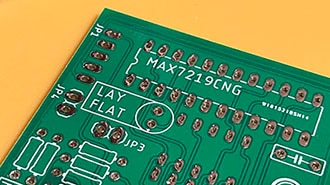
So, what do you need to hand over to the board fab? A digital design file that specifies what should be on each layer, and the shape of the board. So, you’ll need to pick an ECAD software package. KiCad is one popular free option, and you can find a detailed series about using it right here on DigiKey, hosted by Shawn Hymel.
I’m personally more familiar with using Autodesk Fusion Electronics, formerly known as EAGLE. The free version has all the features to create a typical beginner’s two-layer board. The leading professional PCB design software is Altium. You’ll find there are many free tools popping up here and there for PCB design, but they all help you through the same basic steps to design your board.
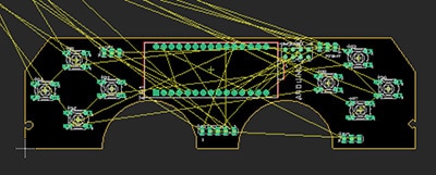
PCB design files all have a schematic and a board layout. The schematic is the circuit diagram, representing the components and their electrical connections to one another in the abstract. The board layout is the physical plan for where components’ footprints are arranged and the individual traces between them.

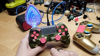
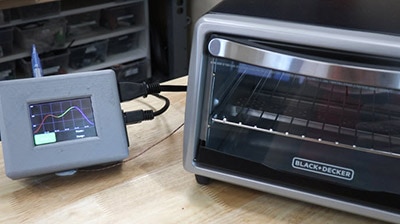
Here’s one of my own circuit board designs: it’s a breakout PCB for the buttons on a Playstation 4 controller. Here’s the schematic view on the left and the board layout on the right.
Your ECAD tool will allow you to specify your circuit board connections in a schematic drawing and then define how they will appear as physical traces on your board. The process of creating the traces and making them all fit together is called routing.
We’re just scratching the surface, but I want to paint a picture of the whole process. A PCB alone doesn’t do anything. It needs components, which need to be attached somehow.


For your first PCB, you might solder your components on yourself. If you plan to go this route, ensure your parts aren’t too small. Surface mount parts can be difficult to solder by hand, even with an appropriately sized soldering iron tip.


One method hobbyists use for tiny parts is a hot air station, to evenly heat all the pads at once. This can be useful because melted solder only likes to flow to other pieces of metal that are also hot. Another DIY PCB soldering method uses a hot plate to heat the entire board at once, which is closer to what happens in commercial manufacturing.

The next step of the commercial process is to apply solder to the pads of the board, which involves squeezing solder paste out through a stencil that’s made to match the board. Then a Pick and Place Machine dispenses the components and sets them down in their proper locations. Then the whole panel goes through a solder reflow oven, which precisely ramps up the temperature to melt the solder paste, and then cools it back down. The solder reflow oven always reminds me of one of those professional bagel or sandwich toasters.
Nowadays you can also easily find a full-service manufacturer who will populate your boards for you too. This is called PCB Assembly, or PCBA for short. You need to send them a BOM, or Bill of Materials, of agreed-upon components that fit the specifications of your design.
In general, when sending work to a factory, it is essential to do your homework upfront. Most of the time, the people making your stuff have no idea what your design does or what's important about it to you, and they often don't even speak the same language as you! So, it's crucial to make it as easy as possible for them to create what you want by communicating clearly and sending them well-formatted, standardized files. Learn more tips in this DigiKey article: The Five Most Important PCB Design Basics Every Maker Must Know.
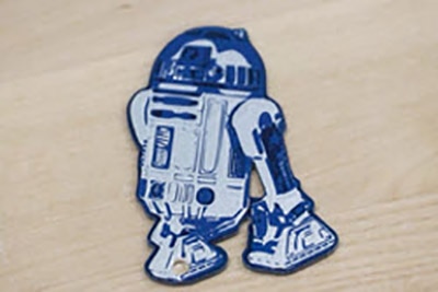
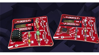
It’s common for your first PCB to be your own version of other people’s designs. The Open-Source Hardware community believes in sharing their board files, so you can find a lot of fantastic free files for all kinds of boards. You can also use the vast library of designs available in the DigiKey reference library.
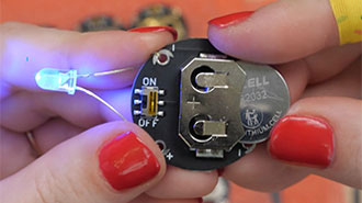
For example, I wanted to make my own version of the open source LilyPad coincell battery holder, so I downloaded the design files, made my own changes, and sent it off for manufacturing.
I hope you’re inspired to try creating your first printed circuit board, or at least come away with a better understanding of the electronic products we use every day. If you’re ready to get started, watch my DigiKey video series from the beginning!