The Five Most Important PCB Design Basics Every Maker Must Know
2024-04-10 | By Maker.io Staff

Creating efficient PCB designs might sometimes seem more like an art form rather than engineering, as spotting a good layout is often easier than creating one from scratch. Newcomers to the maker scene can often find themselves lost in the numerous rules and guidelines to follow before they even start creating a PCB layout, hence why this article summarizes five crucial guidelines for you to keep in mind when creating PCB layouts. This will ensure that you always end up with efficient designs that are also easy to manufacture and assemble.
Consider Component Placement when Designing PCBs
Planning the placement and orientation of components in the design is vital when creating efficient PCB layouts. Many beginners may underestimate the importance of this step, but you should take your time when planning the layout and placing the components on the board.
You should position large parts and components with many connections first. Then, place pairs of components with many adjacent connections close together to reduce the length of signal-transmitting traces and declutter the design. Further, you should account for the space that traces take up on the board and between components, which can be significant. Remember there should always be sufficient space between the traces to account for manufacturing tolerances.
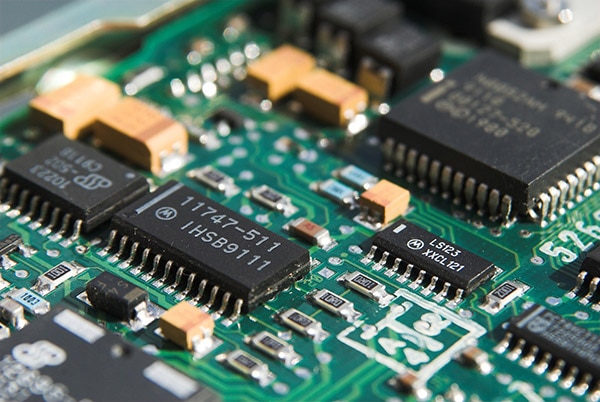
 Consider placing components with many adjacent connections together, for example, different ICs that exchange data.
Finally, separating certain parts of circuits from others may be beneficial or even necessary. For example, a design should keep high-voltage analog sections, such as power supply circuits, away from delicate digital components and pathways to reduce interference and the potential for faults. Similarly, highly sensitive analog circuitry should be kept separate from noisy digital signals to prevent errors.
Harvest the Power of Power Planes
Utilizing power planes instead of traces to supply the components on the board with power prevents the power lines from cluttering up a design and saves precious space on the PCB. A power plane is a large copper area that flows between all other traces on one layer of the board and connects relevant power pins of all components on that layer. Typical maker boards will have two such planes: One that acts as the common ground, and one that supplies the operating voltage — +5V, for example. However, boards with more than two layers could have multiple power and ground planes.
While most beginner projects will not be that power-hungry, power planes can deliver higher currents to a circuit than would be possible using thin traces and can also help cool the entire PCB by offering a large metal surface that acts as a passive heatsink.
Aside from delivering power to the components, such planes are effective in decreasing noise in the circuit; they shorten the ground paths, reduce the inductance, and improve electromagnetic compatibility. Even more so, power planes on both sides of a PCB form a parallel plate decoupling capacitor, which helps prevent electrical noise propagation.
However, keep in mind that designs with sensitive analog components and high-speed digital parts can still benefit from separate ground planes to reduce noise.
Don’t Draw Right-Angle Traces and Avoid Crossing Signals
You should avoid crossing traces on different layers of PCBs to reduce the chance of electrical interference and crosstalk between signals. Each crossing may potentially deteriorate the signal quality and lead to errors in sensitive designs. Placing components carefully or using different pins on devices such as logic gates can prevent most crossings. If two wires must cross, you should ensure they do so at a 90° angle. Similarly, running two traces closely next to each other should be avoided, especially in high-frequency designs.
Finally, you may have difficulty finding a commercially produced PCB that uses 90-degree bends in traces. Instead, you can look for strictly 45-degree bends or curves. While it is true that 90-degree bends might cause problems in very wide traces or extremely high-speed signals, most maker projects will never reach these corner cases. Nevertheless, it’s good design philosophy to keep in line with de-facto standards unless there’s a specific reason to break them. In that sense, you should strive to avoid 90-degree bends in your designs, as they usually take up more space and might confuse others who work with a PCB design.
Make the Layout Easy to Understand and Assemble
In the same sense, the resulting layout should be easy to understand and work with. It’s typically best to keep in line with widely accepted design principles everyone else adheres to. Further, you can utilize component marking and other silkscreen information to add details to your design — to label specific test points, for instance, and help identify critical areas on a board, such as high-voltage sections. You can also add informative labels to your boards, such as version numbers or revision details to make working with the PCB easier.
Use Manufacturer Rules and the Design Tool’s DRC
 Adhere to the manufacturer’s guidelines and tolerances to ensure a trouble-free production process.
Most PCB manufacturers list their manufacturing tolerances on their websites or make them accessible to customers in some other way. These tolerances describe a set of rules a design must follow so that the manufacturer can guarantee good results in the manufacturing process. It’s generally a good idea to follow these guidelines from the very beginning of the design process. For that purpose, most PCB design tools allow you to enter these tolerances so the tool can automatically verify whether a design follows the guidelines. In addition, you should employ the design program’s automated Design Rule Check (DRC) for potential errors in the design, such as missing connections, overlapping traces, or part alignment problems.
Summary
While many projects are simple enough that you may not need to pay close attention to minor details when designing a PCB, it’s still good practice to employ some basic design rules to ensure consistently good results.
You should start by taking your time when laying out the components on the PCB. Place the most important and large parts first to ensure they have space on the board, and then make sure that devices with many adjacent connections are close together. Finally, rotating components can often help reduce the number of crossing traces.
Next, you should separate analog and high-speed digital circuitry to prevent electromagnetic interference from causing errors. Similarly, you can utilize ground and power planes to ensure even power distribution and act as an additional means of reducing noise.
Finally, you should stick to accepted design rules to keep your PCB designs concise. Automated design rule checks can help you find errors in your design and inspect whether the finished design adheres to a manufacturer’s limitations.
Have questions or comments? Continue the conversation on TechForum, DigiKey's online community and technical resource.


