How To Take a PCB Design to the Next Level
2023-10-04 | By Maker.io Staff
Designing a simple PCB can be a relatively straightforward task. Yet, as is often the case, the devil is in the details since a few simple-to-miss oversights can drastically impair the functionality and reliability of a printed circuit board and its electronic components. This article discusses a few methods you can apply to take your PCB layouts to the next level.
Component Placement & Subcircuit Arrangement
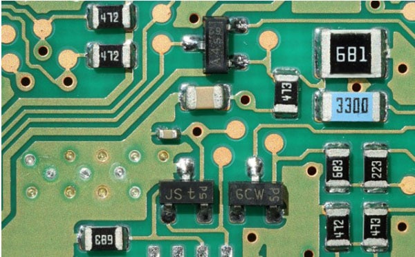
You should not just place components where they fit in a PCB design. Instead, consider relationships between components and arrange them in groups of subcircuits on the PCB to keep connections within groups short. Then, you should identify those components in each group that need external connections to other groups. It’s best to put these parts on the borders of groups to enable trace bundling between adjacent groups. Doing so helps keep the overall PCB design clean and easy to understand, maintain, and troubleshoot.
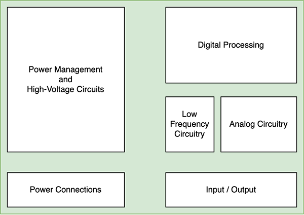 Arrange components within logical groups to help keep connections short and clean.
Following this approach also gives better control over interference. As a designer, you should place noisy, high-frequency subcircuits away from components sensitive to electronic noise, such as analog audio circuitry. Similarly, you should separate power supply circuits from more sensitive parts.
Design Power Supply Rails
Connecting all the signal traces in a design is only half the work, as the components also require power. You can choose from one of two essential ways to connect the power supply rails of a circuit’s components. You can either daisy-chain the power inputs or build a star-shaped topology:
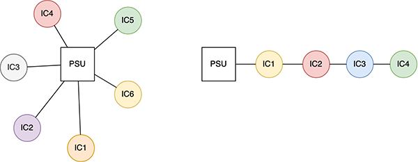 This figure depicts the star topology (left) and a daisy chain (right).
Both approaches offer unique benefits and drawbacks. The star-topology approach generally requires longer power wires while offering better reliability. This design ensures that the other components will still receive power even when one component fails.
In contrast, if one link in the daisy-chain topology fails, the subsequent devices will often no longer receive any power. The current draw of a daisy chain is cumulative, meaning that the current flowing through the first few wires can become very large the longer the chain becomes, which can lead to the trace burning out and failing. Further, a short-term high power draw of one device in the chain may slightly drop the voltage for a brief time, potentially leading to problems further down the chain.
Utilizing power planes is a popular alternative to placing individual power supply wires, especially in designs requiring a single voltage level to operate. Power planes offer a low-impedance way of supplying devices with energy, while also spreading the current load more evenly and dissipating heat more effectively.
Utilizing Ground Planes
Similar to component placement, beginners to PCB design may be inclined to place ground wires wherever they fit. However, when stepping up your PCB design game, you should pay close attention to how you arrange the supply and return paths in your PCB design.
As before, identifying sub-circuits in the overall design can help achieve better results. It’s advisable to keep signal return paths to the ground as short as possible, as short, direct paths minimize inductance and reduce the chance of interference.
Ideally, you want to utilize ground planes in your design, which can split into multiple planes to help isolate sensitive circuitry to prevent crosstalk and interference. Breaking up ground planes is especially important in mixed-signal designs that utilize analog and digital components.
If a design can't accommodate a ground plane, consider connecting the ground traces of each component in a subcircuit into a star pattern to prevent ground loops.
Design for Testability
Unfortunately, not all designs work right out of the box and troubleshooting or tweaking a design is often necessary. However, you can limit frustration in troubleshooting by planning for possible faults and problems when designing your PCB.
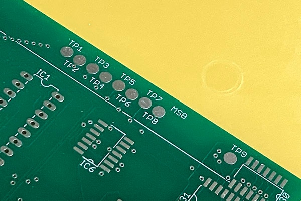 The test points on this PCB help determine the current value of an eight-bit communication bus. The additional silkscreen label clearly marks the most significant bit to further reduce possible confusion when testing.
Adding strategically placed test points to a design is one way of making troubleshooting easier. Test points are specific locations on a PCB that enable convenient testing, debugging, and troubleshooting. They offer easy access to critical signals or components, reducing the need for soldering or probing directly on the board.
Use Silkscreen Markings to Your Advantage
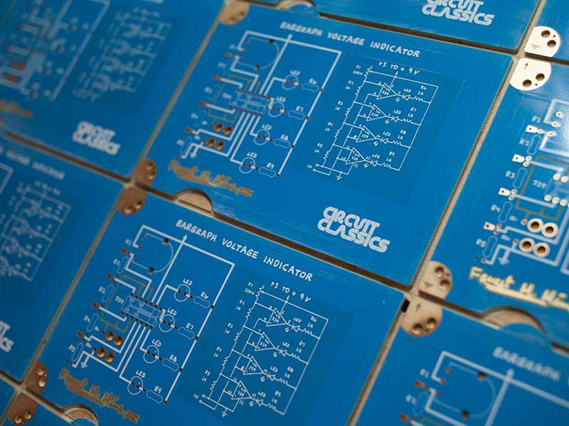
Silkscreen markings are printed labels or symbols on a PCB that provide visual information about component placement, reference designators, and other essential details. In many ways, silkscreen markings are like code comments. While they don’t actively contribute to the functionality of a design, they help others understand the design and reduce confusion.
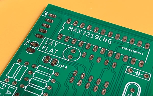 Silkscreen labels can provide the person assembling a PCB with additional information without the need for additional resources, such as a manual.
Descriptive silkscreen labels improve manufacturing accuracy, ensure correct component placement, and simplify troubleshooting and repairs during the product's lifecycle. Silkscreen labels can offer additional information such as expected values, I/O pin labels, board revision information, and much more without requiring additional material such as a printed schematic diagram.
Summary
Component placement is one of the most important steps when designing a PCB. To improve the layout, you should arrange components into logical subgroups to ensure short signal paths between the components of a group. Similarly, parts with connections to other groups should be on the border of their subcircuit, if possible.
Designing a power distribution network can be a tricky task. However, there are generally two approaches that both offer their unique benefits and drawbacks. A star topology network can increase reliability while also generally requiring longer wires. In contrast, daisy-chaining power lines generally lead to a more significant accumulated current draw while reducing the total trace length. Utilizing power planes can be a viable alternative that evenly distributes the current draw and helps dissipate heat.
Similarly, ground planes offer many benefits such as short signal return paths and improved impedance. However, breaking up ground planes is often necessary to improve the circuit’s susceptibility to noise, especially in mixed-signal designs.
Finally, you should consider testability and troubleshooting when designing a printed circuit board. Adding test points to a circuit can help find errors without affecting the circuit, and silkscreen markings can provide vital information when assembling a design.


