Deep Dive into PCB Manufacturing Techniques: Chemical Etching
2024-11-13 | By Jake Hertz
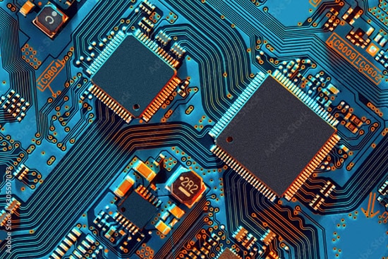
 A PCB layout.
Among the many PCB fabrication methods available, chemical etching remains an industry standard. Known for its precision and scalability, etching offers a reliable method to create detailed circuit patterns. In this blog, we will explore the chemical etching process in detail, as well as its strengths and limitations, and discuss when this technique is most appropriate.
Understanding Chemical Etching
Chemical etching is one of the oldest and most widely used methods of PCB production. The process involves selectively removing unwanted copper from a copper-clad laminate to leave behind the desired circuitry. This is achieved by applying a resist material that protects the areas meant to remain conductive while an etchant solution removes the exposed copper.
 Chemical etching involves chemically dissolving material that is unprotected by photoresist.
The Chemical Etching Process
- Design the PCB Layout: The first step in the process involves creating the circuit design using CAD (Computer-Aided Design) software. The layout must include all traces, vias, and pads necessary for the circuit. Once the design is complete, it is printed onto a transparent film, which will be used to transfer the design to the copper board.
- Prepare the Copper-Clad Board: A copper-clad laminate, usually composed of a fiberglass substrate (such as FR-4) with a layer of copper on one or both sides, is selected. The surface of the copper is cleaned thoroughly to remove any oxidation or contaminants, ensuring proper adhesion of the photoresist layer.
- Apply the Photoresist Layer: The cleaned copper board is coated with a photoresist, which is a light-sensitive material. This can be done by using a photoresist film or by applying liquid photoresist evenly across the board. The photoresist protects the copper in areas where traces will remain.
- Align and Expose the Design: The transparent film containing the circuit design is aligned over the board. The board is then exposed to ultraviolet (UV) light, which hardens the photoresist in the areas where copper needs to remain intact (the traces). Any areas not exposed to UV remain soft and can be washed away later.
- Develop the Board: After exposure, the board is developed using a developer solution, which removes the unhardened photoresist from areas not exposed to UV light. This leaves the desired circuit pattern protected by the hardened resist, while the rest of the copper remains exposed for etching.
- Etch the Board: The developed board is submerged in an etching solution, typically ferric chloride or ammonium persulfate. The etchant dissolves the unprotected copper, leaving only the copper traces covered by the photoresist. This step requires careful control of temperature and time to avoid over-etching or under-etching, which could result in faulty traces.
- Rinse and Remove the Photoresist: Once the unwanted copper is etched away, the board is rinsed thoroughly with water to remove any remaining etching solution. The hardened photoresist is then stripped off using a resist remover or solvent, revealing the clean copper traces that form the circuit.
Why Choose Chemical Etching?
Chemical etching is favored for its scalability and ability to produce PCBs with excellent accuracy, particularly when dealing with intricate designs.
One of its primary advantages is its suitability for multi-layered PCBs. Chemical etching offers superior control, more precise alignment, and higher-quality results across multiple layers when manufacturing boards with more than two layers.
Additionally, chemical etching provides a high degree of flexibility in trace width and spacing, making it a go-to method for high-density interconnect (HDI) PCBs. Whether you’re working with fine pitch components or tight spacing between traces, etching can achieve intricate details that other methods may struggle with.
The technique is also well-suited for mass production. Once the setup and masks are prepared, chemical etching can produce hundreds or thousands of PCBs with minimal variation between them. This scalability, combined with its ability to produce high-quality results, makes it an industry standard for commercial PCB fabrication.
Considerations and Challenges
While chemical etching offers many benefits, it’s important to recognize its drawbacks.
One of the most notable challenges involves the handling and disposal of chemicals. The etching solution, typically composed of ferric chloride or ammonium persulfate, is hazardous and requires proper storage, handling, and disposal procedures. For companies operating at scale, this means investing in safety protocols and environmental compliance, which adds to the overall complexity of the process.
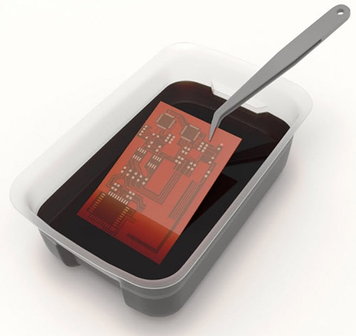
 Chemical etching a PCB.
The process also requires precision in mask application and exposure. Any misalignment or imperfections during the resist application can result in flawed boards. Additionally, over- or under-etching is a potential risk, where either too much copper is removed or not enough, leading to defective traces. Therefore, careful control of etchant concentration, temperature, and time is essential for consistent results.
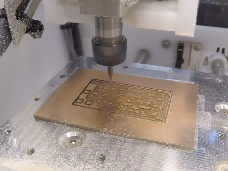
Despite these challenges, chemical etching remains an efficient and effective solution for large-scale PCB production. However, it may not be as cost-effective or practical for small-scale runs or prototyping, where alternative techniques such as milling or direct-write methods may be more advantageous.
Conclusion
Chemical etching is a tried-and-true method for PCB manufacturing, providing a reliable means of producing intricate, multi-layer designs at scale. While the process comes with environmental and operational challenges due to the chemicals involved, its advantages in terms of precision and scalability make it a standard technique in the electronics industry.
Have questions or comments? Continue the conversation on TechForum, DigiKey's online community and technical resource.


