Deep Dive Into PCB Manufacturing Techniques: Milling
2024-10-09 | By Jake Hertz
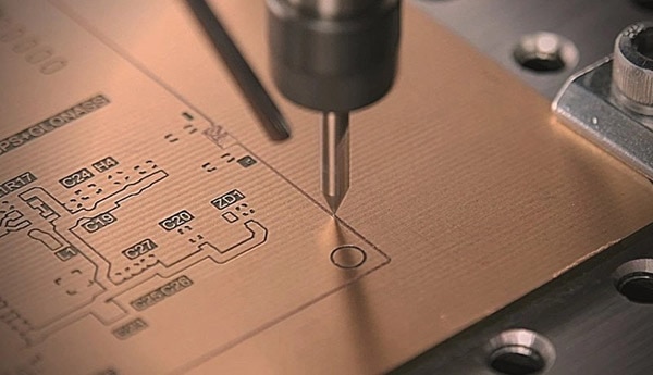
 PCB milling on a board.
Printed Circuit Boards (PCBs) are the backbone of modern electronics, serving as the foundation for nearly all electronic devices. Among the various methods used to produce PCBs, milling is a popular technique, particularly for prototyping and small-scale production. This blog explores the intricacies of PCB milling, the milling process, its advantages, challenges, and applications.
Understanding PCB Milling
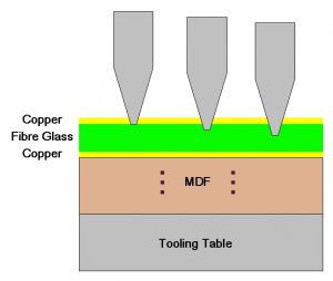
PCB milling involves mechanically removing material from a copper-clad board to create electrical isolation and form circuit patterns. Unlike traditional etching methods, which use chemical solutions to dissolve unwanted copper, milling uses precision-controlled milling bits to physically carve out the desired traces. The process is typically carried out using a Computer Numerical Control (CNC) milling machine, which is programmed to follow a specific design layout to guarantee accuracy and repeatability.

The milling process involves mechanically removing material from a copper-clad board.
The conventional PCB milling process is as follows:
- Design Preparation: The process begins with designing the PCB layout using CAD (Computer-Aided Design) software. This digital design is then converted into G-code, a language understood by CNC machines, which dictates the tool paths for the milling bit.
- Material Selection: A copper-clad laminate, usually FR-4, is selected as the substrate. The thickness of the copper layer is chosen based on the required current-carrying capacity and design specifications.
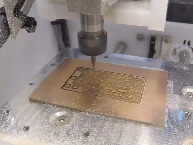
- Milling: The CNC machine, equipped with a high-speed spindle and a micro-milling bit, begins the milling process. The bit follows the tool paths specified in the G-code, removing copper, and creating the circuit traces. The machine's precision allows for intricate designs and fine-pitch components.
- Drilling and Cutting: After milling, the machine drills holes for vias and component leads. The PCB is then cut to the desired shape, completing the manufacturing process.
Advantages of PCB Milling
When considering PCB fabrication techniques, you might wonder why milling is preferred over more conventional methods like etching. Some of the major advantages of milling are:
- Prototyping Efficiency: Milling is particularly advantageous for rapid prototyping. It allows for quick iterations of PCB designs without the need for chemical processing, making it ideal for small production runs or development work.
- No Chemical Waste: Unlike etching, milling does not involve hazardous chemicals, making it a more environmentally friendly option. This also simplifies the setup, as there is no need for waste disposal systems.
- Precision and Control: The CNC milling process offers high precision, with the ability to create fine traces and intricate patterns. This precision is important for high-density designs and modern electronics requiring tight tolerances.
Challenges in PCB Milling
Despite the many benefits of milling, it is not without its challenges. These include:
- Tool Wear and Maintenance: The micro-milling bits used in the process are subject to wear, particularly when milling hard materials or thick copper layers. Regular maintenance and bit replacement are essential to maintain quality and accuracy.
- Surface Finish: Milling can leave burrs or uneven surfaces, which may require additional processing, such as sanding or polishing, to achieve a smooth finish. This consideration applies to high-frequency PCBs where surface roughness can affect signal integrity.
- Limited Layer Count: While milling is excellent for single or double-sided PCBs, it is less suitable for multi-layer boards due to the complexity of aligning and milling multiple layers.
Applications for PCB Milling
Given the advantages and disadvantages of milling, the technique is widely used in scenarios where prototyping is the main objective.
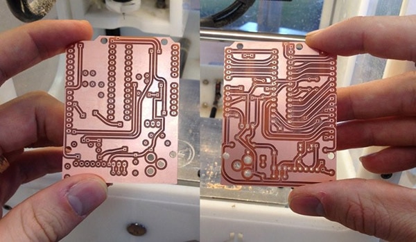
 A double-sided milled PCB.
Engineers often rely on PCB milling to quickly produce and test new designs, iterating as necessary before committing to large-scale manufacturing. Swiftly producing a working PCB can significantly shorten the development cycle and help bring products to market faster.
Additionally, small businesses or hobbyists who need to produce custom PCBs might find milling an accessible and cost-effective solution. Milling provides a practical alternative for projects that don’t justify the setup costs of large-scale production methods.
Conclusion
While PCB milling may not be the best choice for high-volume production, it excels in scenarios requiring rapid prototyping, precision, and environmental friendliness. Understanding when and why to use milling can help you make informed decisions in your PCB manufacturing process and help you select the most appropriate technique for your specific needs.

Have questions or comments? Continue the conversation on TechForum, DigiKey's online community and technical resource.
Visit TechForum


 中国
中国