LTspice Wizardry: Crafting a Full Adder for Digital Circuits!
2024-09-04 | By DWARAKAN RAMANATHAN
Introduction to LTspice:
LTspice is a free circuit simulation software that helps users design and analyze electronic circuits. With this tool, you can visually create circuits and run different types of tests, such as time-based (transient), frequency-based (AC), and steady-state (DC) analyses. It's useful for professional engineers and hobbyists because it makes exploring and fixing circuit designs easier.
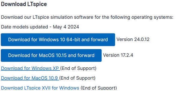
You can download LTspice by Clicking here.
What is a Full Adder?
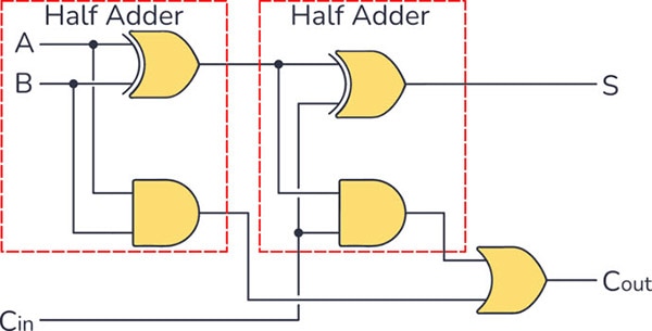
A full adder is a basic digital circuit used to add binary numbers. Unlike a half adder, it can handle three inputs: two binary digits (A and B) and a carry input (Cin) from a previous addition. It produces two outputs: the sum (S) and a carry-out (Cout). The sum is the least significant bit of the result, while the carry-out is the carry generated by adding the three inputs. Full adders are essential for building multi-bit binary adders and other complex digital circuits.
Designing a Full Adder using LTspice:
Step-1: The first step after installing LTspice on your device is to create a new Schematic. To do so, go to File>New Schematic. A new schematic window will be opened for you to add components for your device. Now we will be adding new components to the schematic by clicking on the add components symbol.

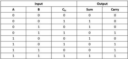
Step-2: For a full adder you will need three types of logic gates (XOR, AND, OR). You can see the truth table and the equations for a full adder's sum and carry below.

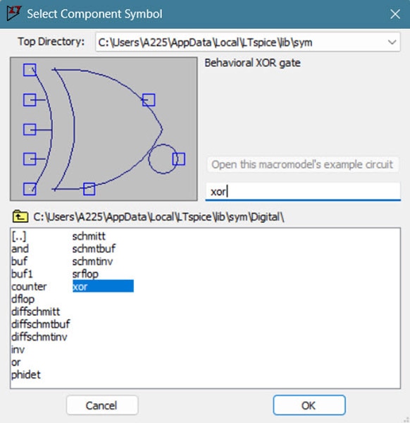
Step-3: We will start adding components, click on the component symbol type xor, and place them as in the circuit diagram above. Do the same for all three types of gates.
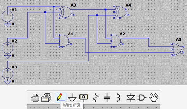
Step-4: It is time to add voltage, so in the same component window type voltage and place three voltages on the left of your circuit for the three inputs (A, B, and C) and connect them using the wire symbol close to the component symbol. Also, connect the ground using the ground symbol next to the wire. Now your circuit should look something like this:
Step-5: Now, it's time to place output pins. To do that, click on the Label Net Symbol near ground, and set the sum and carry to output.

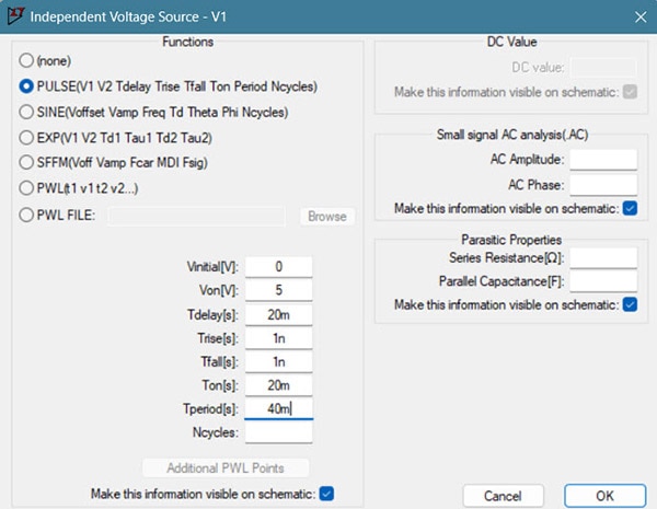
Step-6: Now, we need to configure the input voltage. To do that, right-click on the voltage symbol and click Advanced. Use the values that I have given, and you can try your own values after this. Do the same for all the Inputs with different Ton[s].
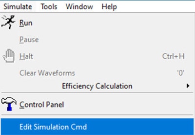
Step-7: Go to simulate and click on Edit Simulate Cmd, set the Stop time to 100ms, then click on OK. Place the .tran 100m somewhere in the Schematic window.
Step-8: Now, it's time to see the output. Go to Simulate and Run the Schematic. You will see a new black pane opened near the schematic window. Go to Window and click on Vertical alignment. Now we have to see 5 different waveforms to check whether the output is correct or not. So, right-click on the black pane and Add Plot Pane.
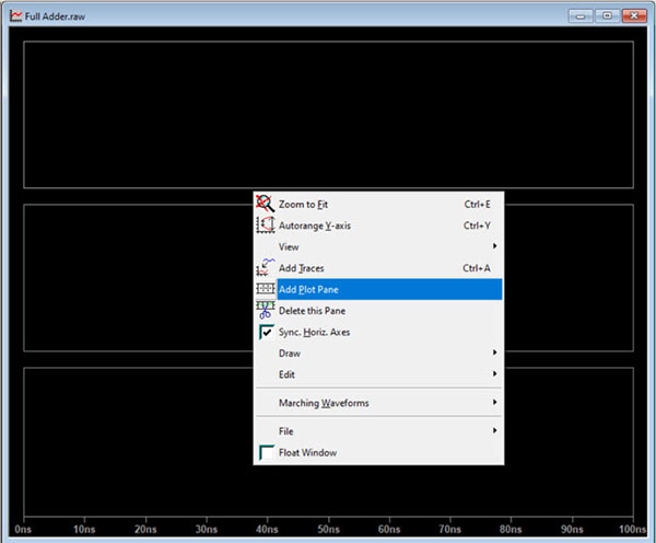
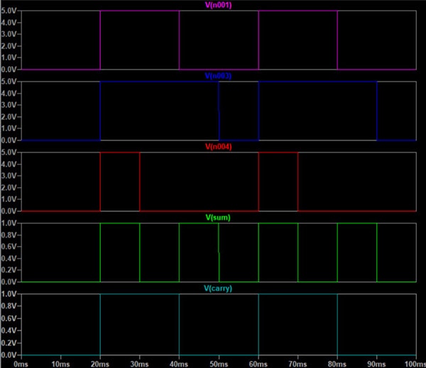
Step-9: Now, click on a single waveform plot pane and click on the wire next to the voltage source to plot the voltage across the wire from the source (Note-If you click on the voltage source you will plot the current in the voltage source, and not the voltage). Finally, you can verify the results with the truth table.
Conclusion:
Designing a full adder circuit in LTspice provides practical insights into digital circuits and simulation techniques. By doing this, you learn the basics of binary addition, the structure of a full adder, and how to use LTspice for circuit simulation. This hands-on experience improves your digital electronics skills and prepares you for real-world engineering challenges.
Have questions or comments? Continue the conversation on TechForum, DigiKey's online community and technical resource.


