Improving the Efficiency of LED Light Emission
投稿人:Convergence Promotions LLC
2011-08-09
Known as electroluminescence, the fortuitous physical phenomenon that allows semiconductor diodes to emit light has created a large industry for LED indicators. But engineers faced a big problem when attempting to boost the light output of LED indicators to make them suitable for general illumination. Only a small percentage of the photons generated actually emitted from the device. The rest were internally reflected and reabsorbed by the crystal, generating unwanted heat.
This article will explain why this problem occurred and the steps high-brightness LED manufacturers are taking to overcome it.
Refractive index mismatch
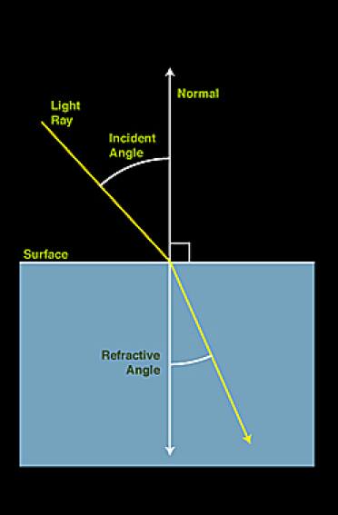
Light travelling through different mediums, such as a semiconductor and air, moves at a different velocity through each medium, causing the light to change directions as it passes from one medium to another. The greater the mismatch in the refractive indices of the two mediums, the more the light bends as it passes through. Figure 1 illustrates this effect.

Figure 1: A light ray bends toward the normal as it enters a material of greater refractive index. The ray bends away from normal when moving into a material of lower refractive index. (Source: Rick Reed)
When light enters a medium of lower refractive index, it bends away from the normal. If the incident angle is large enough, the refractive angle becomes so large that the light ray doesn’t cross the boundary between the two materials, and instead, brings reflected light back in. This situation is known as total internal reflection.
The types of semiconductors used for the photon-emitting element of LEDs (e.g., gallium arsenide (GaAs) and gallium nitride (GaN)) have a high refractive index of approximately 3.7. Air has a refractive index of slightly more than 1. In comparison, diamond has a refractive index of 2.4, and water is 1.3.
Total internal reflection of light can occur with even a small mismatch in the refractive indices of two materials.
Consequently, only a small percentage of the total amount of generated light escapes a thin LED emission layer deposited on a flat substrate. The amount of generated light is slightly larger or about ten percent of the total amount, for a cube-shaped LED. Although there are more faces for a photon to escape in a cube-shaped LED, a light ray reflected from one face is likely to hit another at the same angle and bounce around inside the chip until it’s reabsorbed.
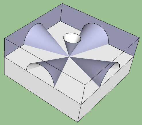
Designers can model the light emission pattern from an LED. Figure 2 shows a typical light emission pattern from a cube-shaped LED with an opaque bottom layer, assuming the light is emitted from a point source at the middle of the chip [1]. In practice, light emission in a cube-shaped LED is more complex than shown in this figure because the light is emitted from a region inside the chip, rather than a point source. As shown, the light is emitted from a small portion of the LED’s surface. The rest of the light is internally reflected and generates unwanted heat.

Figure 2: Light emission cones from a point source in a cube-shaped LED with opaque bottom layer.
Shaping and roughening
Total internal reflection is a major challenge for LED manufacturers when designing LED devices to emit as much light as possible without becoming too hot. Fortunately, there are several techniques for improving the emission efficiency of an LED. The first technique is to change the chip’s shape such that emitted photons are more likely to hit a facet at an angle of incidence close to normal either immediately after emission or after one or two internal reflections.
One way to implement this technique is to change the shape of the die such that different facets aren’t parallel or at right angles to each other. Designers have tested shapes such as triangles, pentagons and octagons. The best light extraction efficiency for a cube-shaped LED is around 13 percent. The best light extraction efficiency for a triangular shaped LED is just over 15 percent. Other shapes result in closer to 20 percent light extraction efficiency.
The ultimate shape is a perfect sphere such that every photon hits the semiconductor and air boundary at a normal angle, at least for the point light source case mentioned above.
Unfortunately, the semiconductor manufacturing process is not suited for making dies in any shape other than cubes because it uses straight saw cuts to remove dies from the wafer. Consequently, manufacturing shaped dies requires an additional manufacturing step, which can become expensive.
A more cost effective and practical alternative is to roughen the upper surface of the die before the individual dies are cut from the wafer. Roughening the upper surface of the die ensures the semiconductor and air boundary comprises thousands of miniature facets at random angles, improving the probability that a photon will approach a boundary at an angle close to normal. According to experiments conducted at Rensselaer Polytechnic Institute [2], roughening the upper surface can increase light emission efficiency from just less than 10 percent to just more than 20 percent.
Manufacturers offer devices with good extraction efficiency by using LEDs with roughened upper surfaces and encapsulating LEDs in epoxy or silicone with domed lenses. We’ll explore encapsulation shortly.
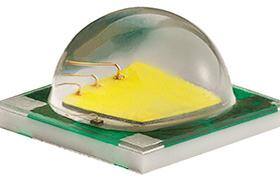
Cree offers its XM-L LED series. These devices are high power LEDs with luminous efficacy values of up to 140 lm/W and are supplied in surface mount packages with domed tops (Figure 3).

OSRAM supplies its OSLON SSL series, which features devices with luminous efficacy values between 70 and 97 lm/W in packages with round lenses and domed tops.
Encapsulation
Another technique that has gained popularity among high brightness LED manufacturers is to encapsulate the LED with a material of a refractive index closer to that of the semiconductor. This can be done during device packaging, and is considerably less expensive than shaping the die.
The closer match in the refractive indices of the semiconductor and the encapsulant means a photon can hit the boundary at a much higher angle of incidence and still be emitted. Consequently, the light cones shown in Figure 1 are much wider, and emission efficiency increases. The photon must pass through a second boundary between the encapsulant and air, but internal reflection is restricted because the boundary is typically dome-shaped. The boundary also often acts as a lens, so virtually all photons hit it at a normal angle.
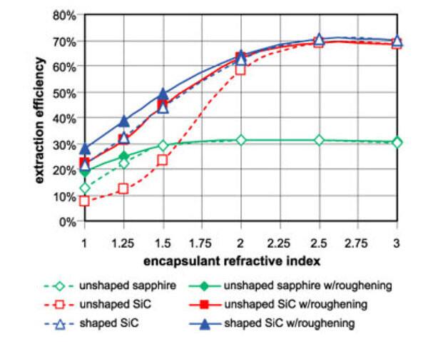
Figure 4 illustrates the extraction efficiency for three chips as a function of encapsulant refractive index with and without top surface roughening. With an encapsulant refractive index of 2.5, extraction efficiency increases to a remarkable 70 percent.

Figure 4: Extraction efficiency for three chips as a function of encapsulant refractive index with and without top surface roughening. (Source: Rensselaer Polytechnic Institute.)
Unfortunately, encapsulants with optimum refractive indices are rare and expensive. Encapsulants that are available commercially, such as epoxy or silicone, have refractive indices of around 1.4 to 1.55. Nonetheless, designers should consider using materials with an unshaped but surface roughened LED chip to increase extraction efficiency to 45 percent.
References:
- “Electroluminescence I,” Gerd Mueller, Academic Press, 2000, ISBN 0127521739, p. 67
- “Extracting more light from LEDs,” Rensselaer Polytechnic Institute, Lighting Research Center.

免责声明:各个作者和/或论坛参与者在本网站发表的观点、看法和意见不代表 DigiKey 的观点、看法和意见,也不代表 DigiKey 官方政策。


