Generating Multiple Voltage Rails from a Single Stepdown Regulator
投稿人:电子产品
2012-12-18
Many system boards require multiple voltage rails to drive a variety of device loads spread across the board. Traditionally, to generate these multiple voltages, designers have been using multiple switching converters or low-dropout regulators (LDOs) to stepdown voltage from the closest supply rail. Besides adding to the cost and taking space on the system board, using multiple switching regulators also requires a separate power stage and loop compensation for each voltage. And using multiple LDOs to stepdown voltages means more power consumption and lower overall efficiency.
An alternative, simple approach is to generate multiple voltages from a single synchronous stepdown regulator using coupled inductors. The outputs can be both isolated and non-isolated. One such design is recommended by Texas Instruments’ application engineer Vijay Choudhary in a design article titled “Simple Stepdown Regulator Generates Multiple Voltage Rails with Good Efficiency and Regulation.”¹ The design uses coupled inductors with a synchronous buck regulator, such as LM5006 to generate auxiliary outputs.
Generating multiple voltages
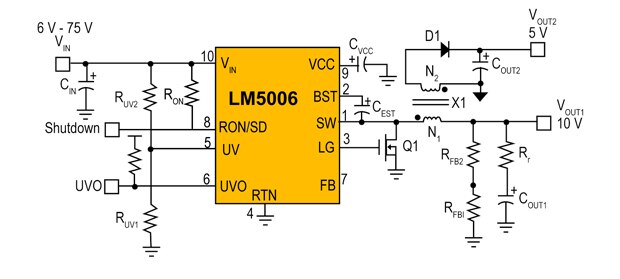
Normally, as shown in Figure 1, to obtain a second output, the primary output is coupled using an inductor and then rectified to get the desired output VOUT2. Although, the concept is simple and provides both isolated and non-isolated outputs, the efficiency drops at lower values of the secondary output voltage VOUT2. The reason given is the diode rectification as depicted in the equation below:

Where N2/N1 is the turns ratio of the coupled inductors and VF is the forward voltage drop of diode D1.

Figure 1: A dual-output, synchronous buck regulator uses coupled inductors and diode rectification.
TI’s application engineer recommends using a high-voltage Schottky barrier diode with minimum loss, such as the Diodes, Inc. DFLS1100-7 for this application. Also, as explained by Choudhary, the flyback action of the diode (D1) causes poor regulation at no load. Consequently, the circuit described in Figure 1 is suitable for applications that require secondary output voltage much higher than the forward voltage drop VF of diode D1. Plus, to avoid a no-load condition, it needs a ballast resistor.
Incidentally, in Figure 1, the rectification MOSFET Q1 used for the primary output VOUT1 is external to synchronous buck regulator LM5006. To eliminate the use of external MOSFETs, TI has readied an integrated synchronous buck regulator, the LM5017. Besides integrating high-side and low-side MOSFETs on-chip, LM5017’s input voltage capability has also been enhanced to 100 V. While LM5006’s input voltage range is 6 to 75 V, the LM5017 offers an input range of 9 to 100 V.
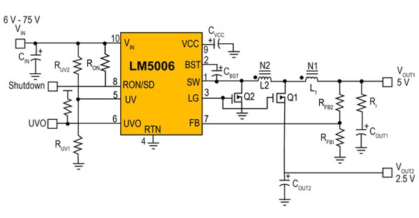
To overcome the limitations of diode D1 in Figure 1, another circuit is proposed that employs coupled inductors with synchronous rectification for both the outputs using the constant-on-time (COT) buck regulator LM5006, illustrated in Figure 2.

Figure 2: A dual output synchronous buck regulator uses synchronous rectification on both output voltage rails.
The result is better efficiency and regulation. Since the COT topology does not require any compensation, significantly less design effort is required to generate multiple output rails that are fairly well regulated, according to Choudhary.
The second output VOUT2 in this dual buck converter circuit is dependent on VOUT1 and coupled inductors L1 and L2 as shown in equation (2) below.

If L1 is assumed to be equal to L2, then VOUT2 = VOUT1/2
However, since the source of MOSFET Q1 is connected to VOUT2, the maximum VOUT2 is limited by the following relationship:
![]()
Where VTH is the gate threshold voltage of Q1, and VCC is the voltage at the VCC pin of the LM5006.
Typically, as explained in Reference 1, VCC is 7.5 V when regulated by the internal startup regulator. If, for example, MOSFET Q1’s threshold VTH is 4 V, the theoretically maximum achievable VOUT2 is VOUT2 (max) = 7.5 V – 4 V = 3.5 V. The designer should take this into account when designing the converter. If a higher VOUT2 is needed, a Q1 with a lower VTH(max) should be selected.
Implementing the techniques discussed above, a dual output working circuit is demonstrated in Figure 3 using the LM5006. As shown, the circuit uses off the shelf 100 µH inductors and low RDS(on) Si2328 MOSFETs fabricated by Vishay Siliconix.

Figure 3: A practical solution for dual-voltage outputs using synchronous buck regulator LM5006.
Internal tests show that load regulation on both the outputs is excellent. In addition, the efficiency performance on the second output VOUT2 remains over 70% from medium to high loads even when the stepdown ratio is high. In this design, VOUT2 is 2.5 V and VOUT1 is 5 V.
Although the design example presented generates only two output voltages, the concept can be extended to generate more than two output voltage rails. As explained in Reference 1, for each added output rail, the circuit would require one additional MOSFET and a winding.
TI recommends these multi-output converter solutions for applications requiring 5 W or less output power.
Reference
- “Simple Stepdown Regulator Generates Multiple Voltage Rails with Good Efficiency and Regulation” by Vijay Choudhary, Texas Instruments, How2Power Today, May 2011.
免责声明:各个作者和/或论坛参与者在本网站发表的观点、看法和意见不代表 DigiKey 的观点、看法和意见,也不代表 DigiKey 官方政策。


 中国
中国