Trade-Offs In Switching High-Input-Voltage Step-Down Converters at High Frequencies
投稿人:电子产品
2013-02-12
In an effort to reduce the size of the output capacitor and inductor to save printed-circuit board (PCB) space, more and more high-input-voltage DC/DC converters are being operated at higher switching frequencies. However, as the output voltage drops to 5 V and lower, designing faster switching high-input-voltage step-down DC/DC converters is becoming difficult for several reasons. Key among them is lower duty cycle.
Consequently, a converter operating at frequencies over 1 MHz impacts the power-supply system in more ways than just its size and efficiency. As a result, there are trade-offs in designing high-switching-frequency DC/DC converters with high-input and low-output voltages. This article examines some design examples that demonstrate the benefits and pitfalls of switching high-input-voltage step-down DC/DC converters at higher frequencies.
To explain these trade-offs, Texas Instruments engineers built three independent power supplies, each operating at switching frequencies of 100, 300, and 750 kHz, respectively. As described in the application note “Challenges of designing high-frequency, high-input-voltage DC/DC converters”,¹ the input voltage for all three DC/DC converter designs is 48 V, while the output voltage is 5 V with an output current of 1 A. According to the designers, such buck converters are typically used for either powering a 5 V logic USB or as an intermediate bus converter to drive other point-of-load (POL) regulators on the circuit board.
Before building the supplies, the engineers established a few design constraints. For instance, the acceptable ripple voltage was set to 1 percent of the output voltage, which in this case amounted to 50 mV. In addition, peak-to-peak inductor current selected was 0.5 A. Each design, which was based on the circuit in Figure 1, incorporates TI’s TPS54160, a 2.5 MHz, 60 V, 1.5 A step-down DC/DC converter with an integrated MOSFET.
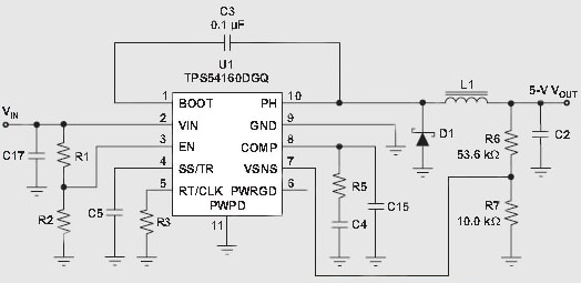
Figure 1: The TPS54160-based high-frequency high-input-voltage step-down converter is used as the reference circuit for evaluating performance of designs operating at three different frequencies.
Selecting filter components
The following equations were used to calculate the value of the output inductor and capacitor for each of the design examples.
For the inductor, V = L × di/dt
The above equation is further reorganized as:

Where duty cycle D = VOUT/VIN = 5-V/48-V = 0.104, ΔI = 0.5 A peak-to-peak, fs is the switching frequency and VDiode is the forward voltage drop in the diode used.
Similarly, for the capacitor,
I = C × dv/dt
Reorganizing the above equation, C is given as

Where ΔI = 0.5 A peak-to-peak, ΔV = 50 mV, and fs is the switching frequency.
In choosing the capacitors for these designs based on Equation 2b, the engineers assumed that the capacitors selected offer negligible equivalent series resistance (ESR), which is true for ceramic capacitors. Hence, because of their low resistance and small size, ceramic capacitors were chosen for all the three designs, as is explained in the application note. Also, TI suggests that the multiplier 2 in the numerator of Equation 2b accounts for the capacitance drop associated with the DC bias. Normally, this effect is not accounted for in the datasheets of most ceramic capacitors, again according to the TI designers.
Using the reference circuit in Figure 1, the designers evaluated the performance of three different solutions, each operating at frequencies of 100, 300, and 750 kHz, respectively. The values for output filter components L1 and C2, which were selected based on calculations using Equations 1a through 2b, are listed in Table 1 along with component size. Since the error amplifier’s compensation components were calculated separately, they are not presented in this discussion.
| Switching Frequency (kHz) | Capacitor C2 (μF/Size) | Capacitor Area (mm²) | Inductor L1 (μH) | Inductor Area (mm²) | Total Area (mm²) |
| 100 | 47/1206 | 18.9 | 100 | 150 | 420 |
| 300 | 10/0805 | 11.5 | 33 | 43.5 | 192 |
| 750 | 4.7/0603 | 6.5 | 15 | 43.5 | 182 |
Table 1: Values of output filter components L1 and C2 for switching frequencies of 100, 300, and 750 kHz, respectively.
Benefits and pitfalls
The minimum output voltage is dependent on the minimum ON time of the DC/DC converter IC and the duty cycle (ratio of the output voltage to the input voltage), so it can be easily calculated. The minimum duty cycle is calculated by multiplying minimum ON time by the switching frequency (Table 2). Once the minimum duty cycle is known, the lowest achievable output voltage can be calculated by multiplying VIN by the minimum duty cycle, as shown in Table 2. It is seen that the lowest output voltage is also limited by the reference voltage of the converter, which is 0.8 V for the TPS54160.
| Switching Frequency | Minimum Duty Cycle | Minimum VOUT at 48 VIN (V) |
| 100 kHz | 0.013 | 0.8 (VREF) |
| 300 kHz | 0.039 | 1.87 |
| 750 kHz | 0.098 | 4.7 |
| 1 MHz | 0.13 | 6 |
Table 2: Minimum output voltage based on 130-ns minimum ON time for switching frequencies of 100 kHz, 300 kHz, 750 kHz, and 1 MHz, respectively.
Table 2 indicates that the designer simply cannot switch at higher frequencies to reduce the size of the components. For instance, the table shows that at 1 MHz switching with 130 ns ON time, the lowest possible output voltage is limited to 6 V. To go below 6 V would mean skipping pulses, which results in higher ripple voltage and noise. In fact, the current-limiting circuit may not work properly because the converter IC may not respond to a large current spike. Consequently, Table 2 suggests that for a 5 V output, the highest frequency that can be used with TPS54160, is 750 kHz. Before selecting a higher switching frequency, TI designers recommend checking the DC/DC converter IC’s datasheet for a guaranteed minimum controllable ON time.
Since efficiency and power dissipation are important aspects of a DC/DC converter design and they are dependent on the switching frequency, power MOSFETs, and the output inductor, the TI engineers carefully examined these features and associated components. They found that overall power loss, which relates to power conversion efficiency, comes from MOSFET driving, switching, and inductor loss. The FET on-resistance and IC loss are consistent since the same IC and MOSFETs are used in all three designs. Because ceramic capacitors with low ESR were chosen in each of the design, the capacitor loss was considered negligible.
Measured efficiency performance for the reference converter circuits switching at three different frequencies is plotted in Figure 2. However, the input voltage in this case is 5 V. The figure suggests that the buck converter efficiency decreases as switching frequency is increased.
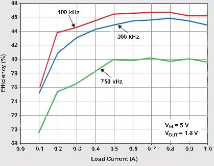
Figure 2: Measured performance shows that the buck converter efficiency decreases as switching frequency is increased for the same input to out voltage ratio.
It should be noted that these efficiency numbers will further decline when the input voltage is higher, especially 48 V because the step ratio now becomes much higher, resulting in more losses at higher switching frequencies. To improve efficiency performance at the desired high frequency, TI recommends using power MOSFETs with very low drain-to-source on resistance, low gate charge, as well as low quiescent-current specification at full load. In addition, utilizing capacitors and inductors with lower ESRs contributes to further cutting losses and enhancing efficiency.
The data presented in Table 1 reflects on capacitor and inductor sizes with respect to frequency. Although, there is a total area savings of almost 250 mm2 between the 100 kHz and 750 kHz designs, providing a 50 percent reduction in filter size and a 55 percent reduction in board space, the law of diminishing returns must be applied. In short, just going higher in frequency does not mean the inductor size will drop accordingly. As this table shows, inductors at 300 kHz and 750 kHz occupy the same area.
Another performance parameter is transient response. Based on the switching frequency, TI engineers have tabulated the actual transient response for the reference converter circuit in Table 3. TI points out that the designer must ensure that the power IC’s error amplifier has enough bandwidth to support a high crossover frequency. In case of TPS54160, the unity-gain bandwidth of the error amplifier is typically 2.7 MHz. Table 3 shows that the transient-response is better at higher frequency with voltage overshoot also lower.
| Switching Frequency (kHz) | Crossover Frequency (kHz) | Phase Margin | Response Time (μs) | Voltage Peak (mV) |
| 100 | 10 | 60° | 1000 | 350 |
| 300 | 30 | 60° | 300 | 300 |
| 750 | 60 | 50° | 150 | 240 |
Table 3: For the reference converter circuit the transient-response is better at higher switching frequency and the voltage overshoot is lower.
Lastly, the TI engineers examined jitter noise, which seems to be a problem at high conversion ratios and higher switching frequencies. Jitter noise becomes a larger percentage of the switching pulse when the duty cycle is small.
In summary, there are trade-offs to designing high-frequency switching converters. While there are some advantages in size, transient response, voltage over- and under-shoots, the pitfalls are reduced efficiency and increased power dissipation, which requires heatsinks or more copper on the PCB. In addition, jitter noise also tends to increase with frequency.
Reference
- Application Note, “Challenges of designing high-frequency, high-input-voltage DC/DC converters,” by Richard Nowakowski, Power Management Product Marketing and Brian King, Applications Engineer, Texas Instruments Inc.
免责声明:各个作者和/或论坛参与者在本网站发表的观点、看法和意见不代表 DigiKey 的观点、看法和意见,也不代表 DigiKey 官方政策。





 中国
中国