Semi-Custom Solutions: Implementing MCU Cores in Programmable Logic
投稿人:电子产品
2014-04-30
There are times when a microcontroller by itself can fully absorb all the functional requirements of a design. For a large majority of embedded system designs, a well-programmed, highly-integrated embedded processor is the most cost-effective, power-efficient, fastest solution available to an engineer.
When raw performance is essential, the captured logic in dedicated hardware achieves the highest level of performance possible. A sequencer, for example, can be an order of magnitude faster than the same logic implemented in software.
Since discrete logic devices take up a lot of space and power, adding an FPGA can be a viable alternative; the combination of FPGA's and microcontrollers is a good solution in many cases. An even denser solution is possible when the micro is implemented in the logic of the FPGA. As a hard-coded macro, or a soft macro that is replaced and routed in every new design, the absorption of the entire microcontroller into the house that is the FPGA can yield not only the highest density, but also the most flexibility, especially if you are brave enough to actually modify the core to improve performance.
This article looks at micro cores that run happily inside readily available FPGAs. These are available from a variety of sources, both open and closed, free, and IP-licensed. All chips, datasheets, reference designs, and development kits discussed in this article are available online on DigiKey’s website.
Better than the original
Both legacy and proprietary architectures can be used, and there are advantages to each. Legacy cores are compatible with legacy micros and provide a familiar architecture. The products your company makes can then use code that is already tested and proven. The reusability of a well-organized and reliable code library can save a lot of time when a next-generation product or even a new and improved model is needed.
Several popular cores have been implemented in raw logic form for a variety of FPGA families including processors such as the Microchip PIC, Intel 8051, Atmel AVR, Motorola 6502, Intel 8080, and Zilog Z80 microcontrollers, to name a few.
A not-so-obvious plus is the ability to improve upon the initial architecture. If time and resources permit, shortcomings can be overcome because you can modify the design. For example, the very popular 8051 architecture was initially introduced with a sequenced architecture that required 12 clock cycles per instruction. Exact legacy implementations can mirror the initial functionality, or can implement more modern flavors that reduced the number of clock cycles per instruction.
Improved IP cores for the 8051 are also available for cross-platform development. The R8051XC2-BF core¹ can be used in an ASIC or with Xilinx and Altera FPGAs; it improves upon the initial design by adding a second data pointer (a shortcoming with the initial design), and a JTAG debug interface (Figure 1).
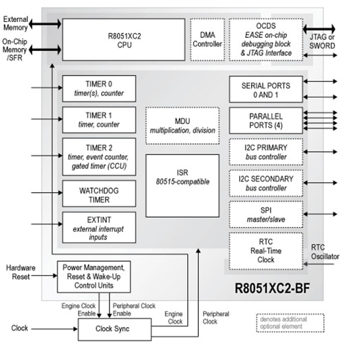
Figure 1: Commercially available implementations of legacy cores often improve upon the initial discrete design. This 8051 core runs at one clock per instruction and adds JTAG and a second data pointer.
ARM cores
While many designs can use 8-bit cores, modern functions can require higher bus widths to streamline processing. If you are manipulating graphics data that is 24 bits wide, a single 32-bit transfer is much more effective than three 8-bit transfers.
Perhaps the most popular 32-bit architecture is the ARM® Cortex™, which to no one’s surprise has become a popular and well-supported architecture for FPGA implementation. The ARM Cortex is very efficient from an area and power usage perspective. The scalable architecture is very well supported by numerous tools and development kits, as well as an open source code for peripherals, memory management, math, and DSP functionality.
A nice feature of the ARM cores is that they are not proprietary to one FPGA maker, and can be implemented on different manufacturers’ devices. This means you are not locked into one supplier as your design evolves or as requirements change.
Another benefit is that the architecture scales from the simpler, less capable Cortex M0 up to very-high-end multi-core A8 and A9 flavors. This also comes with a benefit of track-proven drivers and stacks for higher-end peripherals like USB, Ethernet, Wi-Fi, ZigBee, Bluetooth, and more.
The Xilinx families of parts are big supporters of embedded micro cores, and the ARM architecture is no exception. Parts like the XC5VLX50-1FFG676C are part of the popular Xilinx Virtex® 5 family, and are examples of a very large, dense, and high-end FPGA that can house a fast and dense system on a chip. With 440 I/O and over 46 thousand logic blocks, the 550 MHz parts support not only ARM core functionality, but memory widths up to 72 bits wide, pipelined operations, FIFOs, dual-port memory with up to 16.4 Mbits of internal block memory, and DSP functionality.
Microsemi is another FPGA maker offering ARM core support and the ProASIC3 family is a good target technology with an impressive range of low-to-high-end logic, I/O, RAM, and gate counts from 15,000 to 3,000,000. A good example is the A3PE3000-FGG484 with 341 I/O and 516 Kbits of internal RAM.
Altera has comparable parts like the EP3SL50F780C4N, which similarly supports ARM core processors and also provides memory support for DDR, DDR2, DDR3, SDRAM, and more on up to 24 modular I/O banks with 448 I/O (up to 744 in the family). As a member of the Stratix® III family, Altera provides access to the Altera Mega-Function Partner Program (AMPP) for available peripherals, cores, and support. Altera also supports multiple intellectual properties through its Altera MegaCore functions (Figure 2).
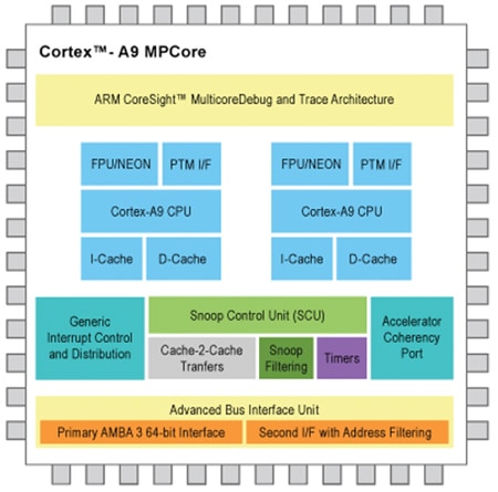
Figure 2: The higher-end 32-bit ARM architecture is a popular core for many FPGAs. This Altera version adds a multicore debug and trace feature, simplifying the design of multiply instantiated processors cores inside a single FPGA.
Proprietary cores
In addition to industry-standard microcontroller cores, FPGA makers also offer proprietary cores that can be very logic efficient and scaled for 8 to 32-bit levels of performance. The key for these suppliers is not to waste logic on un-needed functions and peripherals; so often scaled back, bare-bones processing units are implemented to provide basic programmability and interface to the large pool of logic inside the FPGA. This not only lets the cores operate speedily, but also keeps them small enough to create your own dual-, quad-, or even octal-core processors inside your SoC.
Xilinx designates such cores as Blaze, which is available in both PicoBlaze and MicroBlaze flavors. The PicoBlaze is an 8-bit RISC architecture that has up to 240 MHz performance. It is primarily designed for use in a VHDL design flow and is supplied as a VHDL source file. Once implemented inside one of 13 different Xilinx families, it needs no external components and runs entirely inside the host part.
Families supported include Kinetex-7, Artix-7, Virtex (4,5,6,7, II-Pro), and Spartan® (3 and 6).
From a resource and complexity point of view, PicoBlaze is rather Spartan (pun intended). It features a 16 x byte-wide general-purpose data register, 1K of programmable on-chip program store (automatically loaded during FPGA configuration), a Byte-wide Arithmetic Logic Unit (ALU) with CARRY and ZERO indicator flags, 64-byte internal scratchpad RAM, and 256 input and 256 output ports for easy expansion and enhancement.
On the other hand, it has predictable performance, always two clock cycles per instruction, up to 240 MHz (or 100 MIPS in a Virtex-4 FPGA) and 88 MHz (or 44 MIPS in a Spartan-3 FPGA). PicoBlaze is free to Xilinx users and comes with an assembler and VHDL source code.
On the higher end is the Xilinx MicroBlaze. This is a 32-bit RISC Harvard architecture soft processor core which features 32 general-purpose 32-bit registers, ALU, a rich instruction set optimized for embedded applications, three levels of MMU/MPU support, and more.
The flexibility of this core (Figure 3) allows you to select a performance-optimized five-stage pipeline, which can achieve up to 317 DMIPS with the Kinetix-7 family (such as the XC7K70T-1FBG676C) or a 3-stage pipelined area optimized version that still achieves a respectable 264 DMIPS on Kintex-7 or Virtex-6 and 7 family parts like the XC6VLX130T-1FFG784C.
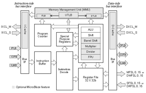
Figure 3: The proprietary 32-bit MicroBlaze core for Xilinx FPGAs has conditional compile directives allowing you to add blocks you need and eliminate blocks you do not to save logic and improve density.
Altera also provides a proprietary core called the NIOS, now in the second-generation NIOS II version (Figure 4). Touted as the most widely used soft processor in the industry, it boasts real-time performance with power sensitivity and safety-critical (DO-254) compliance.
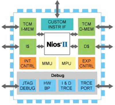
Figure 4: The second-generation NIOS II core from Altera is touted as the most widely used and supported IP core for FPGAs and brings with it a lot of development and debug features.
The six-stage pipelined NIOS cores can be implemented with as few as 600 logic elements and feature vector interrupt control, tight memory and DSP coupling, and the ability to add custom instructions (up to 256 of them). It can use a memory management unit (MMU) and supports embedded Linux in both open-source and commercially supported versions.
A viable alternative
The specifics of your design will determine whether you should select a hard or soft macro. A hard macro takes up specific locations and resources inside the FPGA, but hard-coded macros are better characterized and can achieve better performance.
Soft macros can achieve good performance, too, especially if you are brave enough to modify, improve upon, or parallel them. As always, good design practices will yield the best results.
In conclusion, when the highest possible density and/or performance is necessary, selecting a soft processor inside of an FPGA rather than the traditional microcontroller and all of its support circuitry may be a better solution in terms of flexibility, efficiency, performance, power, and space.
For more information about the parts mentioned in this article, use the links provided to access product information pages on the DigiKey website.
References
免责声明:各个作者和/或论坛参与者在本网站发表的观点、看法和意见不代表 DigiKey 的观点、看法和意见,也不代表 DigiKey 官方政策。




 中国
中国