Simplifying Design with DrGaNPLUS
2016-04-28
This article will address an eGaN FET module designed as a way for power-conversion systems designers to easily evaluate the exceptional performance of gallium nitride transistors.
Simplifying Design
Power converters are constantly trending towards higher output power, higher efficiency, higher power density, higher temperature operation, and higher reliability, all while providing a simpler solution to the designer. The DrGaNPLUS, shown in Figure 1, demonstrates the high-power density capability of eGaN FETs in an easy-to-use building block. With a footprint occupying less real estate than a U.S. penny, the optimized half-bridge design is developed on an 11 mm x 12 mm four-layer printed circuit board (PCB) with mounting pads allowing for connection into any existing converter.

Figure 1: EPC9203 DrGaNPLUS optimized half-bridge building block.
The block diagram of the half-bridge circuit design, shown in Figure 2, consists of two eGaN FETs, a driver integrated circuit (IC), pulse width modulation (PWM) logic, dead-time adjust, and high-frequency input capacitors. The design and layout of these components is critical to fully utilize the high-speed capability of the eGaN FET technology. The DrGaNPLUS gate-drive circuitry ensures the gate-drive requirements for eGaN FETs are met and provides optimized performance with the latest GaN driver IC technology. Users can input two PWM signals to individually control the devices or use the on board logic and dead-time adjust circuit to input a single PWM signal and obtain an optimized dead-time for a buck converter application to maximize performance. The high-frequency input capacitors, also located on board, are arranged with the two eGaN FETs in an optimized PCB layout, minimizing the common source inductance and the high-frequency power commutation loop inductance to decrease switching losses and voltage overshoot. The DrGaNPLUS eliminates complexity and provides the designer an easy-to-use optimized solution with available pads to mount to the PCB, shown on the right in Figure 1.

Figure 2: Block diagram of optimized half-bridge DrGaNPLUS.
Increasing Efficiency
The gains in silicon-based device performance have slowed in the past decade as the technology reaches its theoretical limit, and the package improvements have been limited by the inherent trench structure at higher voltages. This is where GaN transistors come in.
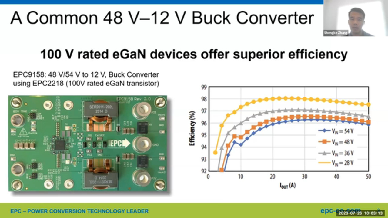
The first commercially available enhancement mode GaN-on-silicon power devices are good potential replacements for the aging power metal-oxide-semiconductor field-effect transistor (MOSFET). eGaN FETs provide lower figures of merit (FOMs) and lower package parasitics which, combined with lower parasitic printed circuit board (PCB) layouts, provide significant performance benefits over state-of-the-art silicon (Si) technology. Shown in Figure 3 is a switching waveform for the EPC9203 DrGaNPLUS module, using 80 V EPC2021 eGaN FETs. The GaN device, with low on-resistance (RDS(on)) and reduced switching charges, enables faster switching speeds and higher operating currents with low voltage overshoot. This enables circuit designers to achieve both lower dynamic-switching losses and lower static-conduction losses, improving converter efficiency. The efficiency of a DrGaNPLUS solution using 80 volt (V) eGaN FETs operating at 300 kHz is shown in Figure 4. With the low-dynamic switching losses provided by eGaN FETs, the switching frequency and power density of the system can be increased without sacrificing performance as shown with the 500 kHz efficiency curve.

Figure 3: Switching node waveforms of eGaN FET design
(VIN = 48 V, VOUT = 12 V, IOUT = 20 A, fsw = 500 kHz).

Figure 4: Efficiency for DrGaNPLUS EPC9203 using 80 V EPC2021 devices at 300 kHz and 500 kHz
There are currently two versions of the DrGaNPLUS module available as noted in Table 1 below. The 40 A EPC9201 uses the 40 V EP2015 and 30 V EPC2023. The 20 A EPC9203 uses the 80 V EPC2021.
| Part Number | VDS (max) | ID (max RMS) | Featured Product |
|---|---|---|---|
| EPC9201 | 30 | 40 | EPC2015/EPC2023 |
| EPC9203 | 80 | 20 | EPC2021 |
Table 1: DrGaNPLUS Part Numbers
Summary
The introduction of high-performance GaN devices offers the potential to switch at higher frequencies and with efficiency than possible with traditional Si MOSFET technology. The eGaN FET-based DrGaNPLUS building block demonstrates the ability to simplify high-power density and high-efficiency power conversion by providing an easy-to-use way for designers to evaluate the exceptional performance of gallium nitride transistors.
免责声明:各个作者和/或论坛参与者在本网站发表的观点、看法和意见不代表 DigiKey 的观点、看法和意见,也不代表 DigiKey 官方政策。


 中国
中国