MCUs Pair with FPGAs to Improve System Efficiency
投稿人:电子产品
2015-05-06
FPGAs have become so cost effective that they are increasingly used in conjunction with MCUs to improve overall system efficiency. Uses include adding extra functionality in a minimum of board space, adding power efficient processing to the front end of complex algorithms, aggregating multiple external devices to offload a high-performance MCU or as the “glue” logic needed to adapt an existing design to new interface requirements, FPGAs provide the additional flexibility often lacking in standard MCUs. This article will quickly review some of the most popular applications where FPGAs and MCUs are “paired” to show how increased system efficiency, via reduced power, reduced board space, improved processing performance, or interface flexibility may be able to dramatically improve your next design.
FPGAs as MCU companion devices
How often does the MCU you have selected for your design just not quite have all the interface channels you require? Or perhaps your initial selection for the MCU fits just perfectly, but a new requirement came along because your best customer wants a few additional interfaces for their newest design. You might be able to use a more complex MCU, but this might result in adding significant board space (because it’s only available in a high pin-count package), increased power (because it’s only available with more flash and SRAM than you really need), or higher cost (for both of the previous reasons).
One way around this dilemma is to plan for the need for additional interfaces by adding an FPGA alongside your MCU. The FPGA can easily provide additional interfaces, and just the ones you need, while limiting increases in board space, cost and power. In fact, when compared to the option of using a more complex MCU, you typically end up with less board space, less cost, and less power.
For example, the Lattice iCE40 ultra-low-power FPGAs can provide up to 26 signal IOs in a very small 2.078 mm by 2.078 mm board footprint, and because these devices are configured via on-chip NVM, you do not require extra board space for a configuration device. These FPGAs also have two dedicated I2C interfaces and two dedicated SPI interfaces with plenty of configurable logic to add as many more interfaces as your application would need (until you run out of pins). A block diagram of the Lattice ICE5LP1K-SWG36ITR50 is shown in Figure 1.
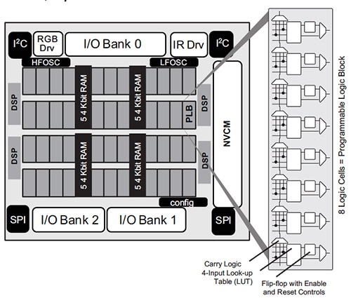
Figure 1: Block Diagram of Lattice iCE5LP FPGA. (Courtesy of Lattice Semiconductor)
The device also has up to 80 kbits of embedded block RAM that can be used for interface FIFOs and buffers so the MCU can wait until an entire data packet is ready for processing. The DSP block can also be used to do low-level data processing on raw sensor data as a pre-processing step prior to sending the data to the MCU. When the FPGA can intelligently aggregate data prior to interrupting the MCU, a dramatic reduction in MCU power is possible. Additionally, Lattice’s iCE5LP FPGAs have been designed for very-low-power applications with a core power supply static current of only 71 μA. Adding more interfaces requires little additional board space or power. Check out the current price difference between your favorite MCU and a higher pin-count version, and then compare it to the Lattice iCE5PL1K FPGA price on the DigiKey website to see what cost savings might also be available.
Responding quickly to FPGA interface requests
When using an FPGA companion device it can be important to respond quickly to the FPGA’s request for service. For example, audio interfaces may need to have higher priority access than sensor data since a “stall” in audio data must be avoided or the user experience could be significantly degraded. In general, being able to support a variety of interrupt priorities can help improve the usefulness of an FPGA companion and further improve overall system performance and power efficiency.
Efficient use of DMA can also help further offload the MCU and improve efficiency. For example, perhaps the FPGA can first buffer up a complete data packet of pre-processed raw data to reduce the size of the message that needs to be stored and transmitted. The FPGA can interrupt the MCU and initiate a DMA transfer that moves the entire message into MCU memory. Once the DMA transfer is complete and the entire message is ready for processing, the CPU can be interrupted and the high-level processing of the message can begin.
The Atmel 32-bit AT32UC3A MCU, for example, has a DMA controller and an interrupt controller, both the programmable priority levels. The interrupt controller diagram, shown on the left side of Figure 2, has a priority block on the right side, which generates the interrupt level to the CPU. The priority block selects the interrupt with the highest priority level, as defined by the interrupt level field in the interrupt priority register (IPRn) associated with each interrupt source. Thus, higher priority sources, for example a real-time audio interface, can be assigned a higher priority than a low-frequency sensor, perhaps on an I2C port, for guaranteed faster processing.
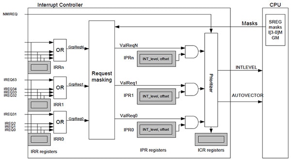
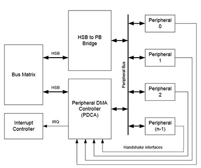
Figure 2: Interrupt Controller and DMA Controller Block Diagrams for the Atmel AT32UC3A MCU. (Courtesy of Atmel)
The AT32UC3A MCU’s DMA controller, the block diagram of which is shown on the right side of Figure 2, connects to many different peripherals, shown on the right side of the DMA block diagram. The peripheral DMA controller prioritizes each peripheral DMA request based on the DMA channel number associated with each peripheral (peripherals are assigned to a channel by a configuration register, so they are fully programmable) with a lower channel number having higher priority. This allows DMA transfers to be easily grouped and optimized for the most efficient data transfer possible. Priority can even be reassigned if sections of the algorithm favor one type of transfer over another.
Sensor fusion further improves system efficiency
As mentioned previously, FPGAs can be used to pre-process sensor data by using DSP techniques. In particular, FPGAs with DSP blocks can implement many common filtering algorithms, such as finite-impulse-response (FIR) filters, infinite-impulse-response (IIR) filters and fast-Fourier transforms (FFTs). Because these hardware blocks can operate either in serial or parallel fashion, you can architect the filter for the optimal configuration based on bandwidth and power requirements. For example, if multiple sensor outputs need to be filtered, the FPGA can either use separate filter blocks for each sensor (if the bandwidth requirement is high enough) or use a single filter block and multiplex it between multiple sensors (if the bandwidth requirement is low enough).
In addition to pre-processing of raw sensor data, the FPGA can also combine readings from multiple sensors, in an intelligent manner to further offload processing requirements of the MCU. Sensor “fusion” algorithms that combine multiple sensor readings locally, prior to informing the MCU that processing is required, can dramatically improve system efficiency. Combining heart rate, temperature, and perspiration readings and comparing the combination against set alarm levels within the FPGA, for example, can provide the MCU with much more valuable information than just raw data.
The MCU typically will need to do some data processing on its own, however. It cannot leave everything up to the FPGA. Luckily, even inexpensive MCUs now have DSP-processing capabilities and can crunch large amounts of data efficiently. The venerable Microchip PIC MCU family, for example, has DSP-oriented family members like the DSPIC 33EP (such as the DSPIC33EP32MC202) that operate at up to 70 MIPS with some instructions performing up to 8 operations at once. Filter-oriented instructions can benefit from the 40-bit accumulator for increased fixed-point precision. A block diagram of the dedicated hardware DSP Engine in the DSPIC33EP is shown in Figure 3.
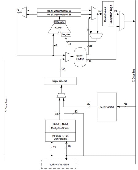
Figure 3: DSP Engine Block Diagram in Microchip DSPIC33 MCU. (Courtesy of Microchip)
The DSP Engine includes a 17 x 17 multiplier/scaler with zero backfill and sign extend to create a 40-bit result. Division operations are implemented via a separate hardware divide block using a repeat loop of 19 iterations, and are interruptible to reduce worst-case interrupt latency. A barrel shifter helps align data correctly for the 40-bit adder and dual 40-bit accumulators. This wealth of DSP-oriented processing hardware is in addition to the regular ALU that provides 16-bit add, subtract, and bit operations. With this extensive set of data processing hardware even complex operations can be supported very efficiently.
SoC FPGAs for hardware acceleration and MCU-based processing
FPGAs and MCUs make such good companions that FPGA vendors are even putting MCU companions on their devices. When these system-on-chip (SoC) FPGAs are used as companions to high-end MCUs, even more complex functions can be moved onto the FPGA. One common example is for the FPGA to handle much of the system interface, not only with standard peripherals but also with external memory. Since SoC FPGAs have significant on-chip memory, an MCU to manage data buffers and process communications frames and an external memory controller, you have all the pieces you need to implement a complete communications channel controller, bridge, or aggregator. This can leave the main MCU to manage higher level functions such as the human machine interface (HMI), process control, and quality of service optimization.
Some SoC FPGAs have additional capabilities that can offload even more low-level processing from the host MCU. For example, the Microsemi SmartFusion2 SoC FPGA family (the block diagram of M2S050-FGG896 is shown in Figure 4), not only has a complete ARM Cortex subsystem, but it has significant on-chip Flash NVM and SRAM blocks as part of the MCU subsystem. These memories can be used in conjunction with the processor, as code and data storage, with the off-chip DDR controller as large buffer memories and with the PCIe and Ethernet controllers as FIFO storage. The intelligent DMA controller can manage much of the data transfer without interrupting the processor.
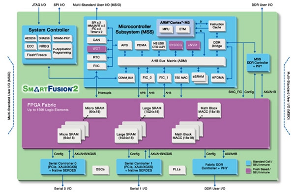
Figure 4: Microsemi SmartFusion2 SoC FPGA Block Diagram. (Courtesy of Microsemi)
SmartFusion2 SoC FPGAs also have on-chip security hardware that can be used to protect remote-code updates from hacking and other security threats. The large on-chip flash memory can be used to store protected boot code, which makes it possible to support secure boot operations, even for a host processor with no native security capabilities. The large amount of programmable fabric can provide custom hardware acceleration to further off-load processing from the host controller. For example, in a chassis control system, programmable fabric can be used for DSP pre-processing of sensor data, sensor fusion combining voltage, current, and temperature readings, motor control of chassis fans controlling system temperature, console interfaces, local diagnostic monitoring and control, or for bridging via PCIe to other control-plane functions. With an SoC the FPGA companion may actually take on more processing than the host, switching the traditional roles between an MCU as the lead actor and an FPGA in only a secondary supporting role.
Conclusion
There are many applications where an MCU and an FPGA, paired together, can dramatically improve system efficiency via lower power, reduced board space, improved processing, or increased flexibility. Knowing how to achieve some of these improvements by allocating functions between these two devices may be the key to success in your next design.
For more information on the parts discussed in this article, use the links provided to access product pages on the DigiKey website.
免责声明:各个作者和/或论坛参与者在本网站发表的观点、看法和意见不代表 DigiKey 的观点、看法和意见,也不代表 DigiKey 官方政策。





 中国
中国