How to Design Wireless Personal Area Networks for Medical and Consumer Applications
投稿人:DigiKey 欧洲编辑
2013-09-05
The range of protocols for ultra-low-power 2.4 GHz personal area network applications such as medical and sports monitoring is expanding, from the Bluetooth Low Energy and ZigBee 802.15.4j standards to proprietary protocols such as Synkro. This article looks at how Bluetooth devices such as the CSR1000 from Cambridge Silicon Radio and the CC2540 from Texas Instruments can be used in medical and consumer designs, as well as the implementation of Atmel’s AT86RF231 and the MC13224 from Freescale Semiconductor for both ZigBee- and Synkro-based networks.
Variations on existing, proven technology are emerging to tackle the challenges of ultra-low-power, short-range wireless networks for medical and consumer use. The well-established ZigBee 802.15.4 standard has been modified to support medical applications in the 2.35 to 2.40 GHz band, adjacent to the existing 2.4 GHz unlicensed band. Single-chip devices for the new Bluetooth Low-Energy protocol are opening up new opportunities to link medical and other consumer equipment to a mobile phone to provide similar personal area networking capabilities.
The medical body area network (MBAN) is one of the key technologies for a personal area network, and the 802.15.4j modification to the ZigBee PHY and MAC was approved in February 2013. This offers the same robust, low-power mesh-networking protocol with a slightly different frequency spread in the US to avoid the crowded unlicensed spectrum, and provide more reliability and robustness in systems from June 2013.
Here the design requirements are less about the data rate and more about the power consumption and cost. Being able to implement a PAN (personal area network) or MBAN with devices that can run for weeks, months, or even years from a single-cell battery is a key aim. 802.15.4j allows devices to operate with lower power as re-transmission of packets is reduced and the shorter range means less power is needed for a link. The mesh networks mean that adjacent devices can be used to carry data across the network, further shortening the link distance and reducing the overall power consumption if there are several sensors across the body. These do, however, need a hub device to control access to the network and to collect data to link to the Internet via networks such as Wi-Fi or a cellular phone. However, the existing ZigBee protocol is also highly applicable to these wearable, personal networks with a low-cost, robust approach.
Bluetooth low energy
Bluetooth has the advantage of connecting to a mobile phone to link personal area network devices to the wider Internet. To do this, the CC2540 from Texas Instruments is a cost-effective, low-power, true system-on-chip (SoC) for Bluetooth low-energy applications. It enables robust BLE master or slave nodes to be built with very low total bill-of-material costs.
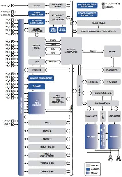
The CC2540 combines an excellent RF transceiver with an industry-standard enhanced 8051 MCU, in-system programmable Flash memory, 8 KB RAM, and very-low-power sleep modes, ideal for medical MBAN. Short transition times between operating modes further enable low-power consumption so the device can power-up quickly, send the data, and power back down again, minimizing the energy used.
The 8051 CPU core is a single-cycle 8051-compatible core. It has three different memory access busses (SFR, DATA, and CODE/XDATA), a debug interface, and an 18-input extended-interrupt unit.

The memory arbiter is at the heart of the system, as it connects the CPU and DMA controller with the physical memories and all peripherals through the SFR bus. The memory arbiter has four memory-access points, access of which can map to one of three physical memories, an SRAM, Flash memory, and XREG/SFR registers. It is responsible for performing arbitration and sequencing between simultaneous memory accesses to the same physical memory.
The SFR bus is a common bus that connects all hardware peripherals to the memory arbiter. The SFR bus in the block diagram in Figure 1 also provides access to the radio registers in the radio register bank, even though these are also mapped into XDATA memory space.
The 8 KB SRAM maps to the DATA memory space and to parts of the XDATA memory spaces. The SRAM is an ultra-low-power SRAM that retains its contents even when the digital part is powered off (power modes 2 and 3).
The 128/256 KB Flash block provides in-circuit programmable non-volatile program memory for the device, and maps into the CODE and XDATA memory spaces.
Writing to the Flash block is performed through a Flash controller that allows page-wise erasure and 4-bytewise programming. See the User Guide for details on the Flash controller. A versatile five-channel DMA controller is available in the system, accesses memory using the XDATA memory space, and has access to all physical memories. Each channel (trigger, priority, transfer mode, addressing mode, source and destination pointers, and transfer count) is configured with DMA descriptors that can be located anywhere in memory. Many of the hardware peripherals (AES core, Flash controller, USARTs, timers, ADC interface, and others) can also be used with the DMA controller for efficient operation by performing data transfers between a single SFR or XREG address and Flash/SRAM.
The interrupt controller services a total of eighteen interrupt sources, divided into six interrupt groups, each of which is associated with one of four interrupt priorities. I/O and sleep-timer interrupt requests are serviced even if the device is in a sleep mode (power modes 1 and 2) by bringing the CC2540 back to the active mode.
The debug interface implements a proprietary two-wire serial interface that is used for in-circuit debugging. Through this debug interface, it is possible to erase or program the entire Flash memory, control which oscillators are enabled, stop and start execution of the user program, execute instructions on the 8051 core, set code breakpoints, and single-step through instructions in the code. Using these techniques, it is possible to perform in-circuit debugging and external Flash programming.
The I/O controller is responsible for all general-purpose I/O pins. The CPU can configure whether peripheral modules control certain pins or whether they are under software control, and if so, whether each pin is configured as an input or output and if a pull-up or pull-down resistor in the pad is connected. Each peripheral that connects to the I/O pins can choose between two different I/O pin locations to ensure flexibility in various applications.
The sleep timer is an ultra-low-power timer that can either use an external 32.768 kHz crystal oscillator or an internal 32.753 kHz RC oscillator. The sleep timer runs continuously in all operating modes except power mode 3. Typical applications of this timer are as a real-time counter or as a wake-up timer to get out of power modes 1 or 2.
Data can be delivered to the transceiver via the ADC, which supports 7 to 12 bits of resolution with a corresponding range of bandwidths from 30 kHz to 4 kHz. DC and audio conversions with up to eight input channels (I/O controller pins) are possible. The inputs can be selected as single-ended or differential. The reference voltage can be internal, AVDD, or a single-ended or differential external signal. The ADC also has a temperature-sensor input channel, which can be useful for medical monitoring to simplify the design of the wireless sensor node. The ADC can automate the process of periodic sampling or conversion over a sequence of channels, relieving the designer of the need to code this.
The operational amplifier is intended to provide front-end buffering and gain for the ADC. Both inputs as well as the output are available on pins, so the feedback network is fully customizable. A chopper-stabilized mode is available for applications that need good accuracy with high gain.
The ultra-low-power analog comparator enables applications to wake up from PM2 or PM3 based on an analog signal. Both inputs are brought out to pins; the reference voltage must be provided externally. The comparator output is connected to the I/O controller interrupt detector and can be treated by the MCU as a regular I/O pin interrupt.
Encrypting the data in the medical network is a key decision for the designer. The data links are very low-power and very short-range and therefore hard to intercept, but ensuring that medical data is secure and safe from hacking is a vital element of any design. ZigBee includes encryption within its protocol, but Bluetooth does not, so there has to be more consideration for implementing data security. The AES encryption/decryption core in the CC2540 allows the user to encrypt and decrypt data using the AES algorithm with 128-bit keys.
Each CC2540 also contains a unique 48-bit IEEE address that can be used as the public device address for a Bluetooth device. Designers are free to use this address, or provide their own, as described in the Bluetooth specification.
ZigBee
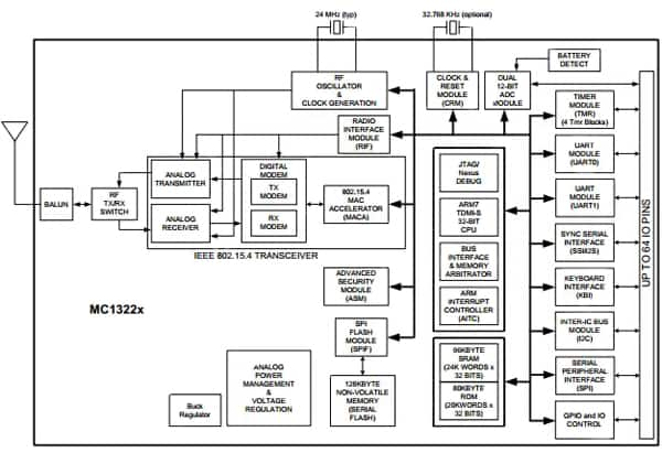
There are several ZigBee devices available that can be used to implement an MBAN. The MC1322x family is Freescale’s third-generation ZigBee platform which incorporates a complete, low-power, 2.4 GHz radio frequency transceiver, 32-bit ARM7 core based MCU, hardware acceleration for both the IEEE 802.15.4 MAC and AES security, and a full set of MCU peripherals into a 99-pin LGA Platform-in-Package (PiP).
The MC1322x can be used for wireless applications ranging from simple point-to-point connections to complete ZigBee mesh. The full 32-bit ARM7TDMI-S core operates up to 26 MHz, while the 128 Kbyte Flash memory is mirrored into a 96 Kbyte RAM so that upper stack and applications software can be easily implemented. In addition, an 80 Kbyte ROM is available for boot software, standardized IEEE 802.15.4 MAC, and communications stack software. A full set of peripherals and Direct Memory Access (DMA) capability for transceiver packet data complement the processor core.

The RF radio interface provides for low cost and the high density as shown in Figure 2. An onboard balun along with a TX/RX switch allows direct connection to a single-ended 50 Ω antenna. The integrated PA provides programmable output power typically from -30 dBm to +4 dBm, and the RX LNA provides -96 dBm sensitivity. In addition, separate complementary PA outputs allow use of an external PA and/or an external LNA for extended range applications, although this is unlikely to be necessary for the short-range MBAN requirements. The device also has onboard bypass capacitors and crystal load capacitors for the smallest footprint in the industry. All components are integrated into the package except the crystal and antenna, allowing the device to be as small and light as possible.
Freescale has two independent codebases to support the two ZigBee standard specifications. BeeStack™ supports ZigBee-2007, ZigBee Pro extensions will support the 802.15.4j-2013 amendments, BeeStack Consumer supports ZigBee RF4CE, and there is also a proprietary Synkro protocol discussed below.
BeeStack
The BeeStack architecture implements the ZigBee-2007 protocol stack including both Stack Profile 1 and Stack Profile 2 (Pro). Based on the OSI Seven-Layer model, the ZigBee stack ensures inter-operability among networked devices. The physical (PHY), media access control (MAC), and network (NWK) layers create the foundation for the application (APL) layers. BeeStack defines additional services to improve the communication between layers of the protocol stack.
At the Application Layer, the application support layer (ASL) facilitates information exchange between the Application Support Sub-Layer (APS) and application objects. Finally, ZigBee Device Objects (ZDO), in addition to other manufacturer-designed applications, allow for a wide range of useful tasks applicable for medical MBAN and consumer-wearable wireless networks.
The key is that the IEEE 802.15.4-compatible MAC/PHY layer is not part of ZigBee itself. The NWK layer defines routing, network creation and configuration, and device synchronization, while the application framework (AF) supports services that define ZigBee functionality. ZigBee Device Objects (ZDO) implement application-level services in all nodes via profiles. A security service provider (SSP) is available to the layers that use encryption (NWK and APS) that rely on the AES 128-bit security.
In addition to the use of two Stack Profiles, ZigBee also embraces the concept of application profiles. The profiles are intended to assure interoperability between like devices for a specific application from different vendors. The application profile specifies a device description and its messaging protocol such that it defines the type, shape, and features of the network. The ZigBee Alliance defines each profile and targets a specific market, and there is a profile for healthcare applications.
Atmel similarly has a low-power 2.4 GHz radio transceiver designed for medical and consumer ZigBee IEEE 802.15.4 designs.
The radio transceiver is a true SPI-to-antenna solution and all the RF-critical components except the antenna, crystal, and de-coupling capacitors are integrated on-chip, making the AT86RF231 particularly suitable for small form factor, low-power MBAN networks.
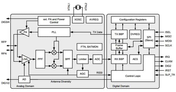
The AT86RF231 can be operated by using an external microcontroller like Atmel's AVR microcontrollers. This single-chip radio transceiver provides a complete radio transceiver interface between an antenna and a microcontroller. It comprises the analog radio, digital modulation, and demodulation including time and frequency synchronization and data buffering. The number of external components is minimized such that only the antenna, the crystal, and decoupling capacitors are required. The bidirectional differential-antenna pins (RFP, RFN) are used for transmission and reception so that no external antenna switch is needed, reducing size and power consumption.

The received RF signal at pins RFN and RFP is differentially fed through the low-noise amplifier (LNA) to the RF filter (PPF) to generate a complex signal, driving the integrated channel filter (BPF). The limiting amplifier provides sufficient gain to drive the succeeding analog-to-digital converter (ADC) and generates a digital RSSI signal. The ADC output signal is sampled by the digital base band receiver (RX BBP). The transmit modulation scheme is offset-QPSK (O-QPSK) with half-sine pulse shaping and 32-length block coding (spreading). The modulation signal is generated in the digital transmitter (TX BBP) and applied to the fractional-N frequency synthesis (PLL), to ensure the coherent phase modulation required for demodulation of O-QPSK signals. The frequency-modulated signal is fed to the power amplifier (PA). A differential pin pair DIG3/DIG4 can be enabled to control an external RF front-end.
An internal 128-byte RAM for RX and TX (Frame Buffer) buffers the data to be transmitted or the received data.
The configuration of the AT86RF231 and the reading and writing of Frame Buffer is controlled by the SPI interface and additional control lines.
The AT86RF231 contains comprehensive hardware-MAC support (Extended Operating Mode) and a security engine (AES) to improve the overall system power efficiency and timing. The stand-alone 128-bit AES engine can be accessed in parallel by all PHY operational transactions and states using the SPI interface, except during SLEEP state. For proprietary applications not necessarily targeting IEEE 802.15.4 compliant networks, the radio transceiver also supports alternative data rates up to 2 Mb/s.
Interfacing the transceiver
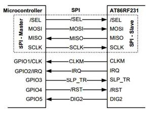
Microcontrollers with a master SPI, such as Atmel's AVR family, interface directly to the AT86RF231. The SPI is used for register, Frame Buffer, SRAM, and AES access. The additional control signals are connected to the GPIO/IRQ interface of the microcontroller. Pin 17 (CLKM) can be used as a microcontroller master clock source. If the microcontroller derives the SPI master clock (SCLK) directly from CLKM, the SPI operates in synchronous mode, otherwise in asynchronous mode.

In synchronous mode, the maximum SCLK frequency is 8 MHz. In asynchronous mode, the maximum SCLK frequency is limited to 7.5 MHz. The signal at pin CLKM is not required to derive SCLK and may be disabled to reduce power consumption and spurious emissions.
Consumer personal networks
Medical personal area networks tend to be driven by the particular needs of a hospital or healthcare service provider, with clear specification and interoperability requirements. There is an emerging sector of the consumer electronics market that is linking devices around the body, providing health information. This can include sensors in running shoes connecting to a phone or a smart watch, or a pedometer or heart-rate sensor linking to a gateway device.
As CSR's first single-mode Bluetooth low-energy solution, CSR µEnergy® enables ultra-low-power connectivity and basic data transfer for applications previously limited by the power consumption, size constraints, and complexity of other wireless standards. The µEnergy platform provides everything required to create a Bluetooth low-energy product with RF, baseband, microcontroller, qualified Bluetooth v4.0 stack, and customer application running on a single chip.
The CSR1000 offers a smaller package for watches and PC mice, providing higher volume and lower cost for fitness products and other wireless sensors.
The CSR1000 includes the Switch-Mode Power Supply and Linear regulators, 10-bit ADC, and three PWM modules, as well as four quadrature decoders. It uses GMSK Modulation for low power and more efficient transmission of data so that less power is used to get data across. This provides ten to twenty times lower power than other schemes such as EDR, as well as using less power to be discoverable and connectable. CSR has developed a low-power Instant Sniff Mode to reduce the power consumption of wireless nodes even further, and the device can make a connection, send data, and get the acknowledgement in just 3 ms.
Synkro RF
There are also other proprietary protocols that can be used for MBAN and consumer PAN networks. SynkroRF is a general-purpose, proprietary networking layer that sits on top of the IEEE 802.15.4 MAC and PHY layers for short distance links in a network. It enables small, power-efficient, inexpensive solutions to be implemented for a wide range of applications. Some key characteristics of a SynkroRF Network are an over-the-air data rate of 250 kbit/s in the 2.4 GHz band equivalent to ZigBee, using three independent communication channels in the 2.4 GHz band (15, 20, and 25), along with a channel-agility mechanism to reduce the impact of other networks. There are two network node types, controller and controlled nodes, with a low-latency transmission mode automatically enabled in conditions of radio interference. A fragmented mode transmission and reception is automatically enabled in conditions of radio interference to allow lower-power links, and includes the essential functions to build and support a consumer electronics personal network. The SynkroRF Network layer uses components from the standard HC(S)08 Freescale platform, which is also used by Freescale’s implementations of 802.15.4 MAC and ZigBee layers and in the MC13224 transceiver.
Conclusion
Keeping the power consumption low is a key requirement for medical personal area networks, and this has to be achieved in potentially noisy RF environments. 802.15.4j moves the frequency spectrum that is available to avoid clashing signals, allowing low-power, short-range devices to operate at the lowest possible power. The alternative approach is to power-up quickly, make a link, and power down, as used by the latest Bluetooth Low-Energy v4.0 protocols. Both have different ways of implementing a system for this fast growing marketplace.

免责声明:各个作者和/或论坛参与者在本网站发表的观点、看法和意见不代表 DigiKey 的观点、看法和意见,也不代表 DigiKey 官方政策。


 中国
中国