The Incredible Shrinking LED
投稿人:电子产品
2015-08-04
Conventional silicon chips have shrunk as wafer fabrication enhancements enable smaller features, thermal management improves, and chip reliability increases. Japanese electronics manufacturer Mitsubishi was the first to launch a Chip-Scale Package (CSP) in 1994. Now CSPs (little more than slivers of the original wafer with minimal additional features) are commonplace. The key advantages of these devices are dramatic space savings, cheaper assembly costs, and improved performance due to factors such as reduced parasitics.
However, until recently, CSPs were not popular for LEDs because of the difficulty in extracting heat from such tiny devices; but increases in efficacy and higher tolerance to temperature (which was the downfall of the previous generation of fragile LEDs) have changed that situation. Now, LED makers such as Cree, Lumileds, and Toshiba have announced commercial CSP LEDs.
This article looks at this recent evolution in LED packaging and leads on to describe how CSP LEDs from leading manufacturers give designers the freedom to come up with new compact form factors that were impractical with the previous generation of LEDs.
Packaging evolution
Moore’s Law, which recently celebrated its 50th anniversary, states that the number of transistors on a chip of given dimensions doubles every 18 months as fabrication techniques improve. However, the law cuts both ways; every 18 months a chip with a consistent number of transistors shrinks to half its previous size. Such component shrinkage is a boon for designers faced with space constraints imposed when designing, for example, wearables.
But reductions in size due to technology improvements have proved insufficient to meet the demand for greater miniaturization. Chipmakers have responded by shrinking the volume of a component still further by systematically stripping away the packaging. The first major move in this direction was to develop surface-mount devices (SMDs). SMDs dispensed with the leads––which went through holes in a PCB to allow a component to both be held in place and make electrical connections––in favor of small pads (Figure 1). The SMD was then “placed” directly onto the surface of the PCB, with reflowed solder paste providing the mechanical and electrical connection, saving considerable space.
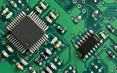
Figure 1: SMD components dispense with through-hole leads and are mounted directly onto the PCB. (Courtesy of Sundeip Arora)
More recently chip vendors have taken things further, removing even the small amount of plastic that encased an SMD such that what is delivered to the customer is little more than bare silicon.
The results can be dramatic. Bluetooth Smart vendor Nordic Semiconductor, a supplier of wireless connectivity solutions used in wearables such as fitness bands, offers two version of its nRF51822 Bluetooth Smart System-on-Chip (SoC). The conventional surface-mount QFN-packaged device measures up at 36 mm2, while the CSP version comes in at 9.6 mm2, a saving of nearly 76 percent in PCB real estate.
Producing a CSP version of conventional ICs is not trivial. It has taken semiconductor vendors many years to perfect the manufacturing processes that allow delivery of reliable slices of silicon that can be bonded to a PCB and resist the stresses of everyday use. But now that the technology is becoming more common, attention has turned to applying the technology to LEDs.
While the majority of LEDs are not manufactured from silicon, rather gallium nitride (GaN) on sapphire or silicon carbide (SiC) substrates (see the TechZone article “Improved Silicon-Substrate LEDs Address High Solid-State Lighting Costs”), they still lend themselves to the same manufacturing processes that have decreased the size of conventional electronics. However, here the process of size reduction for LEDs has been slower because shrinking the chip introduces challenging heat-removal issues.
Heat is the dominant killer of LEDs. The higher the temperature, the sooner the device fails. However, as a large bank of test data has built up over a number of years, it is increasingly apparent that each new generation of devices is becoming more robust and hence capable of lasting longer. For example, even devices operating at a very high junction temperature of 105°C have been shown to routinely last in excess of 36,000 hours.
Smaller is better
The key advantage of CSP LEDs is the obvious one: the technology significantly scales down the size of an LED package (Figure 2); but there are several other upsides. For example, these tiny solid-state lighting (SSL) devices are cheaper to manufacture, allowing the cost savings to be passed on to customers in the form of lower prices.
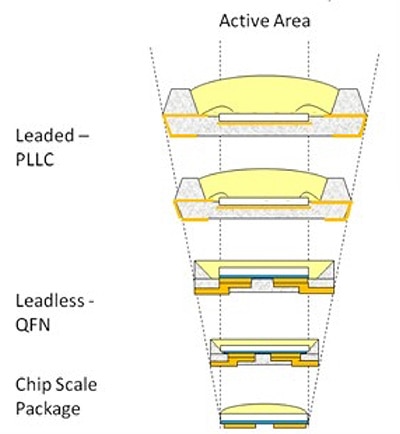
Figure 2: LEDs have progressively shrunk to reach chip-scale package size. (Courtesy of Lumileds)
CSPs take the concept of minimal packaging a step further than even flip-chips by incorporating interconnection pads on the bottom surface of the device on a pitch that matches standard SMDs (Figure 3). This feature does away with the need for the chipmaker to add interposers, sub-mounts, or indeed, any other form of packaging.
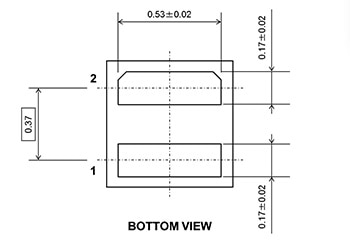
Figure 3: Interconnection pads on the bottom of CSP LEDs match standard SMDs and ease assembly. (Courtesy of Toshiba)
There is no standard definition for a CSP, but the industry generally considers a “chip-scale package LED” to be any device that is equal size or up to 20 percent larger than the active silicon (the light-emitting area of the LED). Devices of this size allow engineers more design flexibility; for example, they provide the freedom to make adjustments in the dimensions of the light-emitting surface and luminance level of the LED, and to shrink the size of lighting fixtures.
Assemblers are also beneficiaries of the inclusion of standard-pitch pitch pads (including both p-type and n-type contacts on the bottom of the LED) because they make the assembly process easier and cheaper. The devices can be mounted directly onto a PCB using standard pick-and-place equipment and there is no requirement for the wire-bonding processes used with other miniature package types such as flip chips. Additionally, CSP LEDs can be tested using standard automatic test equipment (ATE).
Another important advantage of CSPs is lower thermal resistance than conventional LEDs. For example, Toshiba’s TL2F2, a surface-mount LED (producing 136 lm/W [at 65 mA, 2.8 V]) has a package thermal resistance of 30°C/W (from junction to solder interface). In comparison, the company’s TL1WK Series LED (a 112 lm/W [at 60 mA, 2.8 V] device, Figure 4) is available in CSP format and has a package thermal resistance of 17°C/W (again from junction to solder interface). Other CSP LEDs promise thermal resistances down to 5°C/W.
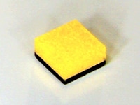
Figure 4: Toshiba’s TL1WK LED exhibits low thermal resistance.
Low thermal resistance allows the LEDs to be driven at higher currents then conventional packages, increasing luminosity, without excessive risk of early failure due to overheating. The low thermal resistance is primarily down to the metal-to-metal interface between the CSP LED and PCB heatsink surface (see the TechZone article “LED Heat Dissipation and Lowering Thermal Resistance of LED Lighting Substrates”).
Because of their small dimensions, CSPs act as a “point light” source rather than the more diffused source from conventionally-packaged products. This makes it possible to use smaller lenses in lighting products using CSPs, lowering the cost and also allowing more compact form factors that were previously not practical. Another optical advantage of CSPs comes from emission of light from five sides of the chip (conventional SMD LED packages emit from the upper face only) which improves luminosity for a given current.
A demand for “lumen density”––which in part has been driven by a need to reduce the number of LEDs for a given light output, in turn pushing down material and assembly costs––is likely to be a catalyst for the uptake of CSP LEDs. The results can be quite dramatic. For example, a typical LED might have a light output of 120 lm, from a light-emitting area of 12.25 mm2 for a lumen density of 9.8 lm/mm2. In comparison, a CSP LED might have a light output of 30 lm, from a light-emitting area of 1 mm2 for a lumen density of 30 lm/mm2 or over three times that of the conventional chip.
Improved lumen density results in smaller, more compact “light engines” comprising fewer LEDs in the active array as well as the development of off-the-shelf Chip-on-Board (CoB) modules, which ease the design of new lighting products for non-expert lighting engineers (see the TechZone article “Maximizing LED Luminosity to Drive Down System Cost”).
CSP LEDs hit the market
There is plenty of activity in the CSP LED sector from the major manufacturers. For example, Samsung Electronics, which owns the Samsung LED brand, introduced its second generation of CSP LEDs in mid 2015. The CSP LEDs are fabricated by flipping over the bare blue LED dies and then applying white-light-emitting phosphor directly to the silicon and all facets of the chip apart from the bottom surface. Because the LEDs do away with any plastic packaging, there was no requirement for molding, simplifying production.
The company’s CSP LEDs measure 1.2 by 1.2 mm (1.44 mm2) and are claimed to offer a 10 percent improvement in efficacy and luminosity over the previous generation (Figure 5). The company will offer the devices as single chips or as two-by-two or three-by-three CSP arrays. The arrays are small enough to share a single lens instead of needing the separate individual lenses used by arrays of conventional LED packages.
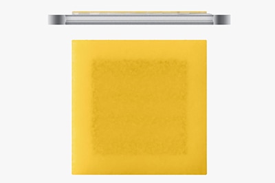
Figure 5: Samsung CSP LED measures 1.44 mm2 in area.
Samsung says the products will be commercially available at the end of 2015. The devices will be available in a range of Correlated Color Temperature (CCT) alternatives specifications.
For now, Samsung offers a range of compact surface-mount LEDs such as the LH351A Series. This chip measures 3.5 by 3.5 mm (12.25 mm2) in area and produces 145 lm/W (at 350 mA, 2.95 V).
Lumileds is also developing CSP LEDs. The 1-by-1 mm chips are in blue LED format only, so lighting manufacturers have to add their own phosphor, and the only addition to the bare die are the pads for soldering. As is usual with blue LEDs, the manufacturer does not offer an output or efficacy figure, but does claim a “wall plug” efficiency of around 60 percent. For the moment the company’s most compact LED-plus-phosphor device is the LUXEON Q, which Lumileds says is based on a “flip chip CSP architecture.” Similar to the Samsung product, LUXEON Q measures up at 3.5 by 3.5 mm and is capable of 124 lm/W (at 350 mA, 2.93 V).
Toshiba already has a CSP LED on the market, the TL1WK chip previously described. The device measures 0.65 by 0.65 mm (0.42 mm2) and can be driven at up to 180 mA without danger of overheating, providing the designer adheres to the company’s recommendations on thermal management.
Cree is also developing a CSP LED, but today its smallest readily available package is the 3.45-by-3.45 mm (11.9 mm2) XLamp XP-E2 LED. This is a 109 lm/W (at 350 mA, 2.9 V) LED and is built on the company’s SC3 technology which uses a silicon-carbide (SiC) substrate.
Set for the mainstream
There is no end in sight in the quest to make electronic components smaller. Compact products such as wearables or sensors for Internet of Things (IoT) applications are driving the demand for greater miniaturization.
LEDs have been slower to shrink than other electronics components because they were prone to failure from the heat generated inside tiny packages, but a push from the lighting industry for cheaper assembly costs and raised lumen density has encouraged LED makers to overcome the technical challenges. Modern chips are much more robust than older devices and are able to withstand the higher temperatures generated by the CSP format (as well as being able to be driven at higher forward currents to boost luminosity).
CSP LEDs are not for everyone; they are fragile and awkward to handle. But the advantages of these tiny packages are many and all major LED manufacturers are working on commercial products for release in the next 6 to 12 months. Analysts are reporting that while CSP LEDs represented only 11 percent of overall high-power LED packaging in 2013, they expect the devices to represent 34 percent by 2020, so expect CSP LEDs to enter the mainstream of LED lighting soon.
For more information about the parts discussed in this article, use the links provided to access product pages on the DigiKey website.
免责声明:各个作者和/或论坛参与者在本网站发表的观点、看法和意见不代表 DigiKey 的观点、看法和意见,也不代表 DigiKey 官方政策。


