How to Select the Right Galvanic Isolation Technology for IoT Sensors
投稿人:DigiKey 北美编辑
2017-12-07
The growth of diverse, new IoT applications has exposed many designers to the challenge of providing galvanic (ohmic) isolation between the sensor and the rest of the electronics. This isolation is critical for signal integrity, system protection, and user safety, but designers have to pick from three main isolation technologies: magnetic, optical, and capacitive barriers.
Each of these options has similar performance characteristics, but have subtle differences that designers need to appreciate before choosing between them. To that end, this article will discuss the role of isolation in sensors, before introducing the various options, their different characteristics, and how to apply them.
It will also introduce digital isolation, and provide further examples of digital isolators.
The essentials of isolation
When a sensor or sensor sub circuit is “isolated”, there is no electrical path between it and the rest of the circuit, and a basic measurement using an ohmmeter would show no current flow between the two sections (Figure 1). As a consequence of this barrier, the challenge is to get signal from the isolated sub circuit to the rest of the system. In many cases, there’s an additional challenge: provide power to the isolated sub circuit without having a “sneak-around path” via the power supply subsystem, which will negate any isolation.
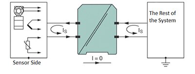
Figure 1: In an isolated system there is no current path between the ungrounded sensor and system (which may be grounded), yet information bearing energy of some type must get from one side to the other. (Image source: DigiKey, based on original material at www.ee.co.za)
Reasons for isolation include:
- The sensor is “floating” and must not have any connection with the system “ground” (system “common” is a more accurate term, but “ground” is the commonly used misnomer here).
- Even if the system is battery operated and so has no connection to “AC ground”, the sensor output may, if it is on top of a high common-mode voltage (CMV). This CMV will damage the rest of the electronics. For example, the voltage of a single battery cell which is at the top of a series stack.
- The sensor may inadvertently get connected to a high-voltage source or even the AC line. This will not only damage the electronics, but also puts users at risk.
Fortunately, there are viable options for implementing analog sensor isolation that provide both low-level and high-level isolation, from tens of volts up to thousands of volts. The latter is needed in mass-market applications such as EV/HEVs, and often for regulatory safety mandates. The three most common approaches for providing isolation use magnetic, optical, and capacitive techniques, with each rated to >1000 V and higher.
These techniques have significant overlap in their primary performance attributes, but also some differences. The decision about which one is most appropriate in the application is often a difficult one.
Among the factors to consider are bandwidth, size and footprint, cost, isolation rating (volts), longevity rating, and personal “comfort.” Finding the right balance of performance parameters depends on the application. Battery monitoring, for example, does not need a fast response, while a high-speed test sensor does.
Magnetic isolation: The starting point
Magnetic-based isolation uses a transformer and is the oldest technique; for many years it was the only technique. The isolation transformer usually has a 1:1 turns ratio and can be fairly small, as it is handing signals rather than power, and dissipation is quite low.
Since a transformer cannot pass DC, nor can it handle very low frequencies well (unless it has a large core), the signal to be isolated cannot be applied directly to the primary (input) side. Instead, the sensor signal is amplified, if need be, and then used to modulate a carrier at much higher frequency (amplitude modulation), or used for pulse-width modulation (PWM).
On the output (secondary) side, the signal is demodulated using conventional techniques to extract and recover the original signal. Isolated power must be provided to the primary side, so there is usually a separate, dedicated, isolated side supply while the output side uses the system rail.
An early drop-in isolated op amp is the AD215 from Analog Devices (Figure 2). Its functionality looks like that of a non-isolated op amp, but it offers 1500 V (rms) isolation and 120 kHz bandwidth. It contains a signal modulator, transformer, and signal demodulator, as well as an isolated DC power supply. All are needed to provide galvanic isolation yet allow analog signals to pass from input side to output side.
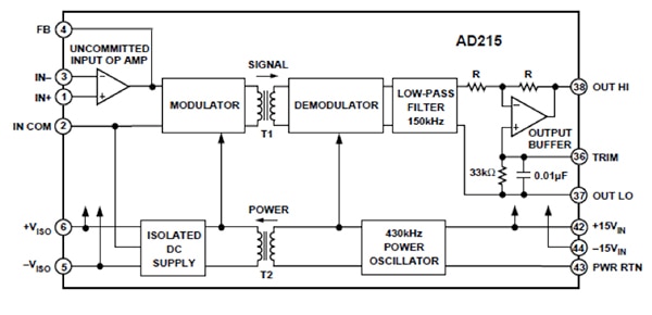
Figure 2: Within the AD215 magnetic isolator are a signal modulator, transformer, and signal demodulator, plus an isolated DC power supply. (Image source: Analog Devices)
The device has a ±10 volt (V) input/output range with a specified gain range of 1 V/V to 10 V/V, and includes an internal, isolated DC/DC power supply for the front end, so no separate supply is required.
Although primarily intended to be used in the feedback loop of switched power supplies, the AD215 can also be used for voltage monitors, motor current sensing, and large battery systems, all of which are well within its 400 kHz bandwidth (Figure 3).
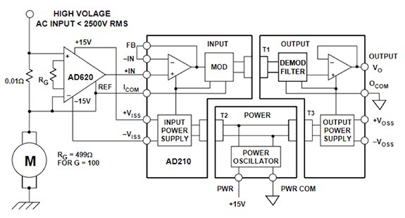
Figure 3: Though primarily intended for use in the feedback loop of switched power supplies, the AD215 also be used for voltage monitors, motor current sensing, and large battery systems. The AD210 shown here is a functionally identical version of the AD215 but with relaxed specifications; the AD620 is a precision instrumentation amplifier. (Image source: Analog Devices)
In such applications, analog isolation is often needed when measuring the voltage across a motor’s sense resistor to determine the current through the motor. This is necessary because the sense resistor is not ground referenced but is instead “floating”, and may be at a very high potential with respect to ground.
These earlier magnetic-based isolation devices used discrete transformers and so were relatively large and expensive. Newer designs use proprietary versions of flat, co-planar transformers that are compatible with IC packaging. For example, the ADuM3190 isolated error amplifier from Analog Devices is housed in a 16-lead QSOP package yet provides a 2.5 kV isolation rating. Its planar transformers are positioned parallel to each other for maximum energy transfer (Figure 4).
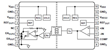
Figure 4: The ADuM3190 isolated error amplifier is packaged to look and handle like an IC, yet contains silicon die and a pair of planar transformers that are positioned parallel to each other for maximum energy transfer. (Image source: Analog Devices)
Although it looks like a standard op amp, it actually takes the input signal and uses it to generate a PWM signal that is passed through the planar transformer. This PWM signal is demodulated and filtered at the secondary side to generate the analog output signal. The data sheet includes standard op amp Bode plots for phase and gain margin (Figure 5). Designers who use this device (or similar ones) can expect to go through standard amplifier loop stability and related modeling and simulation. The Bode plots will help.
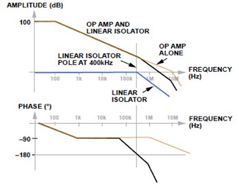
Figure 5: Although it has a complicated, isolated internal architecture, the ADuM3190 from Analog Devices appears to the designer as a conventional op amp. (Image source: Analog Devices)
The ADuM3190 is rated for −40°C to +125°C ambient operating temperature, which is a reality in some of the target applications. Note that since the isolating element is a just wound wire, there is no “wear-out” mechanism in the conventional sense, unless the device is operated beyond its specifications.
However, all insulation materials eventually break down over a sufficiently long period due to voltage stress, with the rate of degradation as a function of the magnitude and type of voltage waveform applied across the voltage barrier. For the ADuM3190, the vendor guarantees a 50 year life even at a maximum rated bipolar AC waveform, which is more stressful than unipolar AC or DC of the same magnitude.
Optical isolation: a newer option
An alternative to magnetic isolation is optical isolation, which is conceptually simple: the input side drives an LED, the output of the LED impinges on a co-packaged phototransistor, and the output is the phototransistor current (Figure 6). The short optical path between LED and phototransistor within the package provides the desired galvanic isolation.
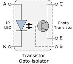
Figure 6: An optoisolator requires two active elements: an LED to source IR, and a phototransistor to convert received photons into electrical current. The galvanic isolation is provided by the optical path within the package. (Image source: Sunpower UK)
As with transformer-based isolation, the input signal is used to modulate the LED current in a digital mode, using PWM or other approaches. The Broadcom (Avago) ACPL-C87B/C87A/C870 family of optical isolation amplifiers is a good example of devices that can be used for voltage sensing across a current sense resistor (Figure 7).
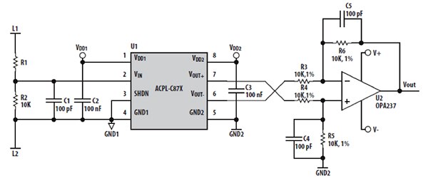
Figure 7: Optoisolators in the Broadcom ACPL-C87B/C87A/C870 family target lower level voltages, and use sigma-delta modulation with a chopper stabilized amplifier for precision, accuracy, and consistency. (Image source: Broadcom)
Isolators in this family have a 2 volt input range and high 1 GΩ input impedance. These specs make them a good fit for isolated voltage sensing requirements in power converter applications, including motor drives and renewable energy systems. The devices combine optical coupling technology along with sigma-delta (Σ-Δ) modulation, chopper stabilized amplifiers, and differential outputs to provide high isolation mode noise rejection, low offset, high gain accuracy and stability. These are all housed in a stretched SO-8 (SSO-8) package.
The devices are well suited to power converter applications due to their 100 kHz bandwidth (Figure 8) and high common-mode transient immunity (15 kV/µs). Such transients are common with motor drives.
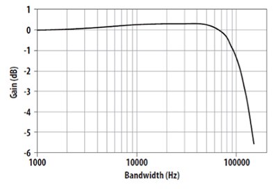
Figure 8: Using its internal sigma-delta analog-to-digital conversion technique, the Broadcom ACPL-C87B/C87A/C870 family of optical isolation amplifiers easily achieves 100 kHz bandwidth with flat response out to 100 kHz. (Image source: Broadcom)
Capacitive isolation: The newest option
Another isolation technique uses capacitance and a minute separation between a capacitor’s “plates” for isolation. The technique has become feasible and cost-effective in recent years due to advances in IC and packaging technologies. A good implementation example is the Texas Instruments ISO124. This is a precision isolation amplifier with its input and output sections galvanically isolated via matched 1 picofarad (pF) capacitors built into the SOIC-16 (or SOIC-18) surface mount plastic package.
Like other analog isolation amplifiers, its high level functional diagram is simple (Figure 9).
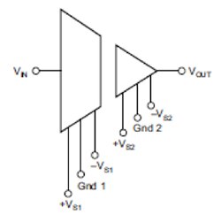
Figure 9: One commonly used symbol for an analog isolation amplifier is this “split” op amp, used on the ISO124 data sheet; this clearly shows that the input and output sections have their own, separate “grounds” (though “common” would be a more correct designation). (Image source: Texas Instruments)
At the same time, the detailed block diagram reveals the complexity of what’s inside and invisible to the user (Figure 10).
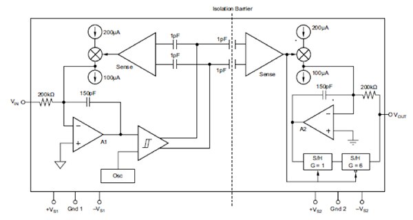
Figure 10: As with the magnetic and optical isolation devices, there is a significant amount of analog and digital circuitry within the ISO124 to make its unique capacitive-based isolation operate. (Image source: Texas Instruments)
The ISO124 input is duty-cycle modulated and transmitted digitally across the barrier. The output section receives the modulated signal, converts it back to an analog voltage and removes the ripple component inherent in the demodulation. It features 0.010% maximum nonlinearity, 50 kHz signal bandwidth, and 200 microvolt (μV)/°C VOS drift, and requires a single power supply between ±4.5 V and ±18 V.
As with non-isolated op amps, the data sheet has both tabular data as well as graphical information on sine wave and step response performance under a variety of conditions (Figure 11). Potential users of these isolation devices need to study the data and diagrams to ensure the device performance is commensurate with the application needs.
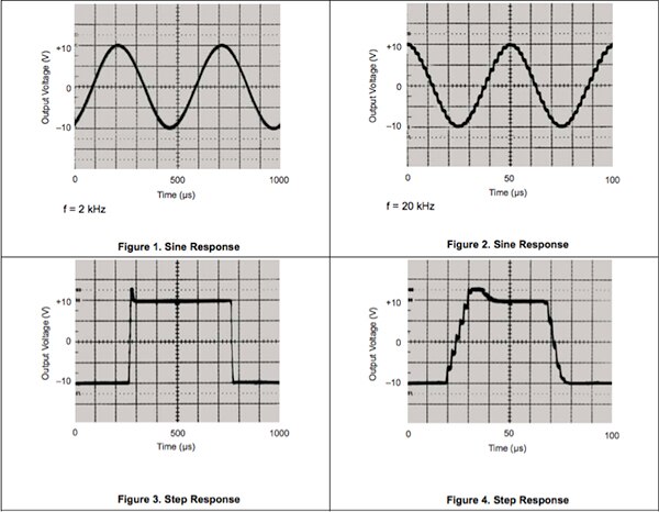
Figure 11: Due to the op amp-like nature of the ISO124 analog-based devices, designers need to pay close attention to the many graphs and tables, including the standard sine and step response graphs. (Image source: Texas Instruments)
The ISO124 is a good fit for low-speed applications, such as isolating the signal from resistance temperature detector (RTD) and thermocouple temperature sensors on a 4-20 mA current loop at the receiver end, and transforming it into a voltage (Figure 12).
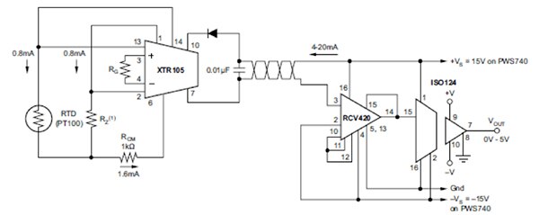
Figure 12: The ISO124 is used to isolate an RTD connected via a standard 4-20 mA current loop, and also convert that current signal into a 0-5 V signal for control system compatibility. (Image source: Texas Instruments)
Temperature measurement applications often require that the sensor be isolated from the rest of the system circuitry due to the potentially high voltage point to which they are directly affixed, such as a motor housing. This voltage is then used by a system analog-to-digital converter (ADC) for readout or closed-loop control, both of which are common industrial situations.
Making the decision
All three analog isolation technologies – magnetic, optical, and capacitive – can provide excellent results under the right conditions. The designer’s dilemma then becomes how to decide on the “best” one in a given situation.
Among the factors to consider are bandwidth, expected lifetime (time to failure or wear out), size, and power requirements. Each isolation technology balances these attributes and may offer specific products with different tradeoffs within a family, thus complicating the decision.
Regarding the amount of voltage isolation, all three types are certified to at least 1 kV (some go to 5 kV and even higher) and meet relevant regulatory standards (IEEE, VDE, CIE, UL, CSA). Therefore, maximum isolation voltage is not an issue for most IoT applications. If this should become an issue, specialty isolators are available which are certified for higher voltages.
There are some general statements that can be made about each isolation technology, but for each statement there are exceptions, and vendors of each technology make effective and legitimate arguments as to why their approach is better. In general:
Magnetic isolation has very long life and its passive barrier can withstand surges and spikes that are much greater than the continuous voltage rating. However, due to its inductive coupling via magnetic fields, it can be susceptible to interference from external magnetic fields. Some of the newer designs successfully minimize this issue to such a degree that the units are certified against such interference susceptibility using industry standard tests.
Optical isolation has high immunity to electrical and magnetic noise, but has modest speed due to LED switching speed, higher power dissipation, and concerns about LED wear. The last issue is the most serious one, as LEDs do experience degradation (dimming) in normal use, with typical half-brightness periods of about ten years. However, companies such as Broadcom/Avago have pushed the state-of-the art in LED materials and so are guaranteed to meet specifications for twenty years, which is often sufficient for the situation.
Capacitive isolation has high immunity to magnetic noise, and compared to optical isolation, it can support wider bandwidth because there are no LEDs that need to be switched. In reality, most IoT sensor applications are low bandwidth situations. Capacitive coupling also involves the use of electric fields for data transmission, so it can be susceptible to interference from external electric fields.
Analog versus digital isolation
Thus far, we have looked at analog isolation techniques for IoT sensors (Figure 13).
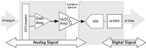
Figure 13: In the analog isolation topology, the sensor signal remains as analog information (regardless of what happens within the isolator itself) until it reaches the non-isolated side, where it can be converted to digital format for further use. (Image source: National Instruments)
However, there is a fundamental architectural alternative: digital isolation, where the analog sensor’s output is conditioned and digitized on the isolated side, and the digital output is then passed through a digital isolation barrier (Figure 14).
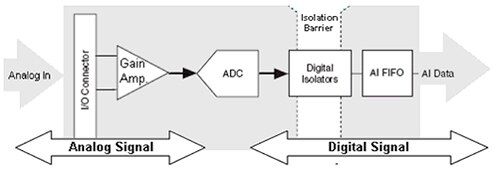
Figure 14: An alternate and often attractive approach is to digitize the signal on the isolated side, then pass the conversion result through a digital isolation barrier. This allows for a very different isolation function implementation, compared to an analog isolation design. (Image source: National Instruments)
As with analog isolation, this barrier can use any of the three technologies, but their internal design is optimized specifically for digital signals and can usually support data at tens of Mbps. Further, for digital isolation there is a new, fourth category option that uses a modulated RF carrier instead of modulated (LED) light. The Si863x series from Silicon Labs is a good example of such a device (Figure 15).
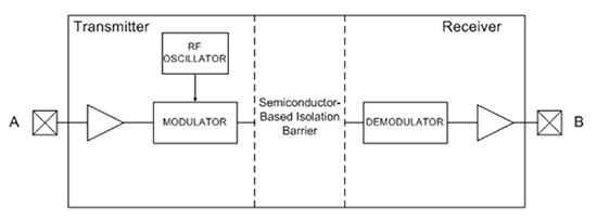
Figure 15: The Si863x series of digital isolators from Silicon Labs use a modulated RF carrier instead of light to carry the signal while providing isolation. (Image source: Silicon Labs)
As the cost of ADCs has gone down, and vendors have standardized around interfaces such as I2C and LVDS, the use of digital isolation becomes more attractive. The downside is that more circuitry is required on the isolated side. This means that more isolated power is needed, adding to cost and footprint.
Once again, though, advances in lower power high-performance ADCs are making this less of a problem. Standard interface digital isolators, such as the 1 MHz ADUM1250 for I2C and 600 Mbit/sec ADN4651 for LVDS, both from Analog Devices, simplify this design alternative. There are also ADCs with integral isolation in their multi-chip IC package, such as the 16-bit Analog Devices AD7401A which make the entire conversion and isolation process transparent to the user.
Finally, there’s the issue of multichannel isolation. While many IoT applications have just one or two sensors that need isolation, others may have four, eight, or more. In those cases, the individual analog isolators in aggregate may be too large, costly, and power hungry,
An alternative approach is to use a multichannel ADC or a single channel device with a front-end multiplexer, all on the isolated side, with higher speed digital isolation to transfer the results. This may be more power, space, and cost-effective than simple per channel isolation.
Conclusion
Analog sensor isolation is a critical issue in many IoT applications for signal integrity, system safety, and user protection. Three viable competing technologies can implement isolation, each offering many similarities in performance but with some subtle differences. Digital isolation, with sensor digitization on the isolated side, is also an option to consider in many applications.

免责声明:各个作者和/或论坛参与者在本网站发表的观点、看法和意见不代表 DigiKey 的观点、看法和意见,也不代表 DigiKey 官方政策。


