Generating Negative Output from Positive Input Voltage
投稿人:电子产品
2012-10-16
There are some applications, such as double-ended sensors and audio amplifiers that require a negative voltage for operation. With limited space on today’s system boards, creating a dedicated negative supply rail would add to the cost and space of the PCB. Hence, it makes sense to generate the required negative voltage from existing positive supply rails in the system.
One such solution using a traditional synchronous step-down regulator is provided by Texas Instruments in an application note entitled “Creating an Inverting Power Supply Using a Synchronous Step-Down Regulator"1. It shows you how to generate a negative voltage from a positive input voltage to the synchronous buck regulator.
Before presenting the design, the author discusses the benefits of using a synchronous topology versus non-synchronous circuit. One of the key benefits of using a synchronous design is higher conversion efficiency at low voltages. Also, a synchronous topology stays in continuous conduction mode (CCM) even at very low currents as opposed to a non-synchronous topology that goes into discontinuous conduction mode (DCM) when the current through the power supply inductor is reduced to zero. Some other disadvantages for a non-synchronous topology in DCM mode are slow transient response, and slower compensation for the DCM shift. Plus, it requires additional components on the board. These disadvantages can be eliminated by using a synchronous topology.
Negative converter solutions
There are some design restrictions that the engineer must observe in order to create an inverting supply from a positive rail. As shown in Table 1, the maximum allowable output voltage is limited by the maximum voltage across the device VDEV between the input pin and the ground (GND) pin on the IC minus the maximum input voltage VIN (max). Because the MOSFETs are internal to the IC, the maximum load current cannot be more than the maximum current through the internal switches.
| Inverting Power Supply Restrictions | Synchronous Device Used | TPS54620 | |
| Vin (min) | > | Vdev (min) | 4.5 V |
| Vin (max) + Vout | < | Vdev (max) | 17 V |
| Iout (max) | < | Iswitch (max) | 7 A |
Table 1: Minimum inverter requirements.
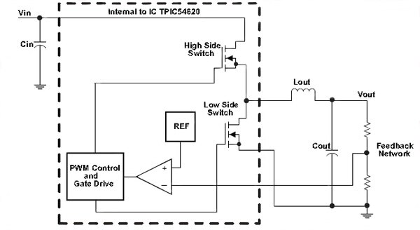
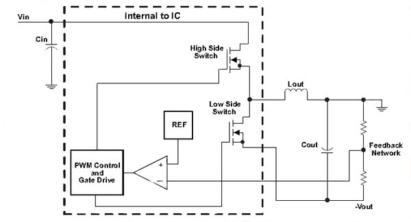
Now, to convert a synchronous buck regulator (Figure 1) into an inverter with negative output voltage, TI suggests that the inductor and the output capacitor be kept in the same locations as in the original buck converter circuit, but the ground and output voltage points must be reversed in order to achieve a negative output voltage, as shown in Figure 2.

Figure 1: Synchronous buck regulator circuit (Courtesy of TI).

Figure 2: Negative output voltage converter wherein ground and voltage output Vout are reversed (Courtesy of TI).
In fact, TI illustrates the concept by implementing the above technique using its chip TPS54620, which is a 4.5-V to 17-V input, 6-A synchronous step-down converter belonging to TI’s SWIFT family. The key electrical specs for this design are depicted in Table 2. While the complete inverter solution using the TI chip is shown in Figure 3.
| Variable | Description | Range / Value |
| Vin | Input Voltage | 5 V nominal 4.5 V to 5.5 V |
| Vout | Output Voltage | -5 V |
| Vout | Output Voltage Ripple | <0.5% |
| Iout | Output Current | 2 A |
| fsw | Switching Frequency | 300 kHz |
Table 2: Key specs for the inverter circuit in Figure 3.

Figure 3: Inverter solution using the TI chip TPS54620 (Courtesy of TI).
The design must ensure that the minimum and maximum input voltages are as per the requirements listed above in Table 1, while the difference between the maximum input voltage VIN (max) and the output voltage Vout must not exceed the maximum operating device voltage of the regulator. For the TPS54620, the maximum operating device voltage VDEV (max) is 17 V.
Now let’s look at two relevant equations:
![]() (1)
(1)
![]() (2)
(2)
The VOUT for this inverter circuit is -5 V. Hence, using Equation 1, it is determined that the maximum input voltage for the power supply can be as high as 12 V. While the minimum input voltage VIN (min) for the inverter supply must be greater than the minimum device voltage VDEV (min). For TPS54620, the VDEV (min) is 4.5 V. Hence, the input range of 4.5 to 5.5 V, as given in Table 2, is easily supported by the TPS54620-based inverter circuit in Figure 3.
Also, using Equation 2, R4 can be calculated for the desired output voltage. In this example, R5 is set equal to 10 kΩ and VREF to 0.8 V. Consequently, using Equation 2, R4 is then calculated to be 52.5 kΩ. A standard value of 52.3 kΩ is recommended instead.
The TI application note also shows you how to calculate other parameters for this inverter circuit, such as duty cycle, output current, operating frequency, inductor value, output and input capacitors, and power dissipation.
Likewise, a new generation of Linear Technology’s high-voltage synchronous step-down converters, such as the LT3845, make it possible to implement positive-to-negative converters for a variety of applications. Linear’s design note 433 entitled “A Positive-to-Negative Voltage Converter Can Be Used for Stable Outputs Even with a Widely Varying Input”2 describes a design example that shows how to generate negative voltage from a positive input to synchronous step-down controller LT3854. In this example, the synchronous controller converts 9- to 15-V wide input to -12 V at 30-A output.
Charge pump inverters
Charge pumps offer a simple, inductorless DC/DC converter solution that can step up, step down, or invert an input voltage for a variety of low-power, low-cost applications. By eliminating the inductor, these switched-capacitor based converters provide compact simple designs for converting positive input to negative output.
Maxim Integrated offers a variety of charge pumps, generating negative voltages from positive inputs for a number of applications. The supplier’s Application Note 7823 illustrates a negative voltage inverter using the MAX1681.
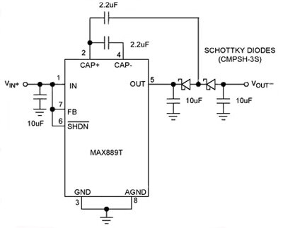
Another Application Note (36594) from Maxim presents a charge pump converter circuit that produces -10 V at no load with more than 200 mA from +5-V input. The charge pump IC used in this circuit is MAX889 as shown in Figure 4. It inverts the input voltage and doubles the resulting negative output at the same time. For that, it uses two Schottky diodes and the two capacitors at the output to produce a higher output voltage as shown in the figure.

Figure 4: Charge pump IC MAX889 inverts the positive input voltage and doubles the resulting negative output at the same time (Courtesy of Maxim).
Summary
For some applications in which only a positive supply is available, the system must generate a negative voltage (sometimes of even larger magnitude than the positive rail). This article discussed how to create a negative power supply using either a switching regulator (buck) or a charge pump. Schematics were presented along with equations, so that designers can determine the best solution to meet their own requirements. The application notes referenced also include sample design implementations along with captured waveforms. For more information on the parts mentioned, use the provided links to access product information pages on the DigiKey website.
References
- Application Report “Creating an Inverting Power Supply Using a Synchronous Step-Down Regulator”, by Sureena Gupta, Texas Instruments
- “A Positive-to-Negative Voltage Converter Can Be Used for Stable Outputs Even with a Widely Varying Input” by Victor Khasiev, Design Note 433, Linear Technology Corp.
- Maxim Application Note 782 “Charge Pump Doubles Negative Voltage”
- Maxim Application Note 3659 “Simple Circuit Converts +5V to -10V”
免责声明:各个作者和/或论坛参与者在本网站发表的观点、看法和意见不代表 DigiKey 的观点、看法和意见,也不代表 DigiKey 官方政策。


 中国
中国