Charge Pumps Tackle Higher-Voltage Applications
投稿人:电子产品
2013-03-26
In their most basic form, charge pumps are circuits that generate a voltage larger than the supply voltage from which they operate. Traditionally, charge pumps have been perceived to have limited voltage capability, offering performance that is seen as filling a niche in the range between low-dropout LDOs and switching regulators. Nonetheless, there are benefits that make them attractive for certain applications. For instance, charge pumps deliver higher efficiency with good thermal management and have the flexibility to step up a voltage, step it down, or invert the input voltage. Since they use capacitors to store and transfer energy, charge pumps also are simple to design and do not require an inductor, which can be more costly, has higher output-noise levels, and frequently lowers output-current capability.
With advances in process technology, manufacturers have improved the input-voltage capability of these devices. Integrated charge pump circuits now are capable of driving low-noise, high-voltage operational amplifiers (op amps). They also can be used to deliver bipolar supplies from a single supply to power dual-rail high-voltage op amps. They can generate sufficient power to drive the white LEDs used for backlighting LCD panels.
To address the needs of a variety of applications requiring high voltage without inductors, suppliers including Linear Technology and Maxim Integrated, among others, have readied a broad series of charge pumps. Since charge pump outputs are not well regulated, some suppliers offer regulated charge pumps that are the byproduct of integrating on-chip a low-dropout regulator (LDO).
Typical examples
Linear Technology, for example, has developed two high voltage inverting monolithic charge pump ICs, the LTC3260 and LTC3261, for these applications.¹ The LTC3261 is a high voltage inverting charge pump that can deliver up to 100 mA of output current, while the LTC3260 is an inverting charge pump that includes on-chip both positive and negative LDO regulators that can source up to 50 mA output current each.
The negative LDO post regulator is powered from the inverting charge pump output. The positive and negative LDO output voltages can be adjusted down to 1.2 and -1.2 V, respectively, using external resistor dividers. Both devices operate over a wide input voltage range of 4.5 to 32 V.
A typical application circuit generating ±12 V from a 15 V input is illustrated in Figure 1. As shown, it uses a few external resistors and ceramic capacitors for stability. Plus, the LTC3260 IC features soft-start circuitry to prevent excessive current flow during startup, and incorporates short circuit and thermal protection. The part comes in a low-profile 14-lead DFN package and a 16-lead MSOP package, both with a backside thermal pad. Operating junction temperature for the device is –40° to +125°C.
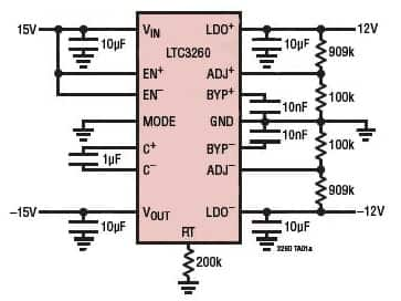
Linear Technology points out that the charge pump employs either low quiescent current Burst Mode operation or low-noise constant-frequency mode at up to 88% efficiency. In Burst Mode operation, the charge pump VOUT regulates to –0.94 VIN and draws only 100 μA of quiescent current with both LDO regulators on. In constant frequency mode, the charge pump produces an output equal to -VIN and operates at a fixed 500 kHz or to a programmed value between 50 kHz to 500 kHz using an external resistor.
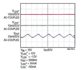
Designed for low-noise performance, the charge pump’s high operating frequency leads to a low output ripple. The LTC3260 LDOs further minimize this ripple (Figure 2) to deliver very low-noise outputs of <1mVp-p that are ideal for noise sensitive applications such as operational amplifiers and analog-to-digital converter (ADC) drivers.
The LTC3261, which is a subset of LTC3260, comes in a 12-lead MSOP package with backside thermal pad and operating junction temperature of –40° to +125°C.
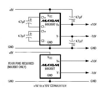
Another manufacturer supplying high-voltage charge pumps is Maxim Integrated. The company is offering its MAX680/81 CMOS based monolithic dual charge-pump converters, capable of generating ±10 V outputs from a +5 V input voltage. For that, they are designed to provide both a positive step-up charge pump to develop +10 V from +5 V input and an inverting charge pump to generate the –10 V output. Both the parts incorporate an on-chip 8 kHz oscillator. While MAX681 offers the capacitors internal to the package, MAX680 requires four external capacitors to produce both positive and negative voltages from a single supply (Figure 3).
For applications that demand smaller packages and smaller capacitors, Maxim is recommending MAX865 in ultra-small μMAX package with switching frequency over 20 kHz. For powering analog functions, it provides positive and negative outputs that are two times the positive input.
An additional high-voltage charge pump in Maxim’s arsenal is MAX1822. It is crafted to generate a regulated output voltage that is 11 V greater than the input supply voltage to power high-side switching and control circuits. The operating supply voltage range for MAX1822 is 3.5 to 16.5 V.
Charge pumps are also tailored for driving white LEDs with constant current for uniform intensity. For that, Maxim has readied a high-efficiency inverting charge pump with extremely low-dropout adaptive current regulators. Designated MAX8647/48, it can drive up to six white LEDs or two sets of RGB LEDs with regulated constant current for display backlight and fun light applications (Figure 4). Maxim reports that the part offers very high efficiency over the full 1-cell Li-ion battery voltage range, even with large LED forward voltage mismatch. The 1 MHz fixed-frequency switching allows for tiny external components. Furthermore, the regulation is optimized to ensure low EMI and low input ripple.
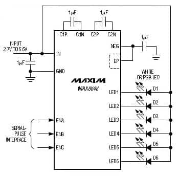
The device is offered with an I²C serial port or three-wire serial-pulse logic interface. It provides independent on/off and dimming for main and sub-backlights. Also, the dimming ranges are pseudo-logarithmic from 24 to 0.1 mA and off in 32 steps. In addition, the inverting charge pump ICs include a temperature derating function to safely allow bright, 24 mA full-scale output current setting while automatically reducing current to protect LEDs at high ambient temperatures above +60°C. The part comes in a 16-pin, 3 x 3 mm thin QFN package.
Summary
Charge pumps are a simple, low-cost, compact power supply alternative to inductor-based designs. Suppliers offer a wide selection of parts that can be used to step-up, step-down or invert an input voltage. By eliminating the inductor, these switched capacitor converters provided a small solution footprint. Recent developments enable designers to provide sufficient power to drive multiple LEDs from a single-cell Li-ion battery or power source, using charge pump technology.
For more information on the high-voltage charge pumps mentioned in this article use the links provided to access product pages on the DigiKey website.
Reference
- Design Note 507 “High Voltage Inverting Charge Pump Produces Low Noise Positive and Negative Supplies” by Marty Merchant, Linear Technology
免责声明:各个作者和/或论坛参与者在本网站发表的观点、看法和意见不代表 DigiKey 的观点、看法和意见,也不代表 DigiKey 官方政策。




 中国
中国