Design Tips for Generating Split-Rail Power Supplies
投稿人:电子产品
2013-01-15
Many analog functions in industrial and medical applications, such as amplifiers, sensors, data converters and other such circuits, require both positive and negative supply voltages to operate. Normally, such circuits require ±5 V, ±12 V, ±15 V, or higher voltages. However, while positive voltages are common on a typical printed-circuit board (PCB), generating negative voltage becomes challenging when the power required is more than 1 W and the supply must be isolated.
To simplify such a task, semiconductor suppliers such as Texas Instruments, Maxim Integrated Products, and Linear Technology, among others, have generated designs using their respective converter chips or modules. One such circuit is presented in an application note written by Texas Instruments Product Marketing Manager Rich Nowakowski.¹
It describes techniques for generating split-rail power supplies from a single, integrated, wide input step-down converter such as the company’s TPS54060, which is a 60 V, 0.5 A buck regulator with an integrated high-side MOSFET. For higher output current with dual isolated output voltages, TI presents a split-rail solution using company’s fly-buck DC/DC converter TPS55010 and an off the shelf transformer. The half-bridge power stage comprising high- and low-side FETs are integrated in the same package.
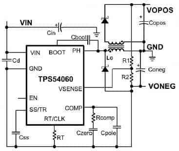
Figure 1 shows a circuit for generating both positive and negative output voltages using an inverting buck-boost topology with a transformer-coupled split-rail design. The design is implemented using the step-down DC/DC converter TPS54060A, a 60 V, 0.5 A buck regulator with an integrated high-side MOSFET. Aside from generating the split voltages, the DC/DC converter is also configured to regulate the positive voltage and uses the secondary winding to regulate the negative output.

The ground pin of the step-down converter TPS54060 is connected to the negative output, VONEG, and the positive lead of the output capacitor is connected to ground. The output voltage VONEG is adjusted by selecting the values of the resistor divider R1 and R2. The transformer’s primary-side output voltage is reflected to the secondary-side. Because the polarity of the primary and secondary windings is opposite, a positive secondary-side voltage is generated from a negative primary-side voltage.
Using this circuit, designers have generated ±18 V at up to 100 mA. Equations used to calculate the values of components used in this design are presented in the application note SLVA369A.² Other output voltages can be generated by changing the values of the converter’s resistor divider. The design example provides up to 100 mA for the positive and negative output voltages.
There are several manufacturers that offer off-the-shelf coupled inductors in a variety of standard values, saturation currents, and sizes. The converter uses external compensation for stability optimization and an integrated power MOSFET to reduce the total parts count. Besides the inductor and the DC/DC converter, the other main external components are two power diodes, along with ceramic input and output capacitors. The remaining components are small resistors and capacitors that configure the DC/DC converter. This solution does not provide isolation between the input and the output.
Isolated split-rail voltages
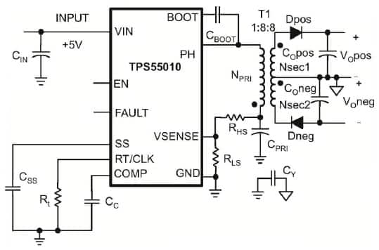
For applications that require isolated split-rail voltages, Nowakowski presents a circuit using a fly-buck converter, which is a variation of a flyback topology and integrates a power stage with high- and low-side power MOSFETs. What is more, it is transformer driven to provide isolated dual output voltages. As illustrated in Figure 2, positive and negative outputs are generated using the fly-buck converter TPS55010 with a 2 μH transformer using a 1:8:8 turns-ratio to provide both ±15 V outputs at 40 mA, each from a 5 V input source. The regulation accuracy of both outputs is mainly dependent on the transformer, low-side MOSFET, and the diode losses. Therefore, the output voltage-drop increases as the output current increases, which tends to limit the maximum output power for a given output voltage.

An advantage of the fly-buck converter is that the input and output are isolated through the transformer’s magnetic coupling. Additionally, substantial cost is saved due to the absence of an optocoupler, since primary-side feedback is used. Further, the output power stage is integrated to eliminate the use of external power MOSFETs.
The voltage on the primary-side capacitor is regulated by the controller and this voltage is reflected to the output through the transformer. The output voltage of the fly-buck is determined by the turns-ratio of the transformer and the voltage divider resistor values on the VSENSE pin, which provides many options for selecting the output voltage.
Similarly, for generating isolated ±12 V at 40 mA from +5 V input, Linear Technology is recommending its LT3574, an isolated flyback converter. The part senses the isolated output voltage directly from the primary side flyback waveform and does not require an optoisolator for regulation.
Generating ± voltages from a battery
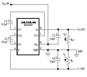
Many battery-powered products, such as handheld instruments, data acquisition systems, and panel meters, need ±6 V from a 3 V lithium battery, while analog circuits require ±10 V from a standard available +5 V logic supply. For such applications requiring low-current, Maxim Integrated Products has readied monolithic CMOS dual charge-pump voltage converters such as the MAX680/MAX681. As depicted in Figure 3, the monolithic voltage converters provide both a positive step-up charge pump to develop +10 V from +5 V input, and an inverting charge pump to generate the –10 V output. Both parts have an on-chip 8 kHz oscillator. While MAX681 has the capacitors internal to the package, MAX680 requires four external capacitors to produce both positive and negative voltages from a single supply. Inexpensive electrolytic capacitors are used in this example.

The output source impedance is typically 150 Ω, providing useful output currents up to 10 mA. The low quiescent current and high efficiency make this device suitable for a variety of applications that need both positive and negative voltages generated from a single supply.
Maxim also recommends MAX865 for designs that prefer to switch at higher frequencies. The device operates from 200 to 400 kHz and uses smaller capacitors.
References
- “Techniques For Implementing A Positive And Negative Output Voltage For Industrial And Medical Equipment,” by Rich Nowakowski, Texas Instruments, How2Power Today, October 2012.
- Application note SLVA369A, “Creating a Split-Rail Power Supply With a Wide Input Voltage Buck Regulator,” Revised October 2012.
免责声明:各个作者和/或论坛参与者在本网站发表的观点、看法和意见不代表 DigiKey 的观点、看法和意见,也不代表 DigiKey 官方政策。


 中国
中国