Choosing Peripherals and Integrated Memory in Microcontrollers for Wearable Designs
投稿人:电子产品
2014-09-24
A new generation of wearable technology is being enabled by highly integrated system-on-chip (SoC) designs. The latest 32-bit microcontroller cores from ARM and MIPS are providing high performance with support for new operating systems such as Android Wear and adding a wide range of peripherals to support new displays, interactive interfaces and sensor applications.
The move to 32-bit cores allows high-level development tools to be used not just for user applications, but also for the management of the whole design, particularly for power management of the peripherals. Being able to implement complex algorithms to optimize the power consumption is vital to get the best possible battery life, and this is closely coupled with the peripherals implemented in the system-on-chip devices at the heart of wearable designs.

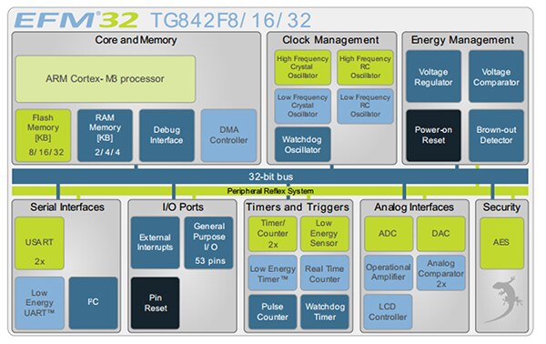
Figure 1: The Tiny Gecko EFM32TG842 from Silicon Labs is aimed directly at wearable designs through its peripherals.
The choice of the processor core architecture is often down to the experience of the system architect and the design team, as well as strategic corporate relationships. There are many designers adept at developing on both the ARM and MIPS platforms, using high level C development tools and the peripheral management tools that come with each of the different silicon suppliers.
Devices such as Silicon Labs' Tiny Gecko EFM32TG842 with a central ARM Cortex-M3 processor core (shown in Figure 1) are aimed directly at wearable designs with a small size and low power consumption but also a range of peripherals optimized for such applications. Freescale Semiconductor also has a range of system-on-chip devices based on the ARM Cortex-M0+ devices in its KL16 family that are part of its WaRP wearable development platform.
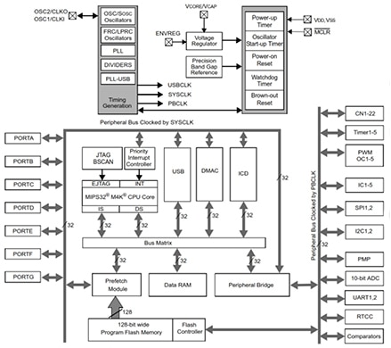
Similarly the PIC32MX340F512H-80I/PT SoC from Microchip Technology uses the MIPS M4K core running at 80 MHz (Figure 2).
While the core speed is relevant, it does not tell the whole story. Many of the peripherals can run independently of the core, delivering more performance than the headline clock rate would imply. This allows the current consumption to be kept low, and there are peripheral management blocks that allow the data transfers to be handled without any CPU intervention. There is also a wider range of general-purpose I/O pins and the choice of pin-out is very much dependent on the selection of internal peripherals and the chosen features of the design.

Figure 2: The Microchip PIC32MX340F512H-80I/PT runs at 80 MHz with a wide range of peripherals.
There is also a wide range of memory options. Balancing the Flash memory required to store and update the code with fast SRAM and on-chip DRAM for execution depends very much on the application, but can also be influenced by the choice of system-on-chip. The peripheral management systems and integrated sensor interfaces can reduce the code requirements for the central CPU, reducing the demand on the memory footprint. Compact instruction sets and compilers can also reduce the memory requirements, but this is balanced by the increasing use of standard libraries that are not optimized for the hardware platforms. Therefore there is tremendous focus on choosing the right set of peripherals to deliver the applications within the power, memory and system cost limitations.
Energy management
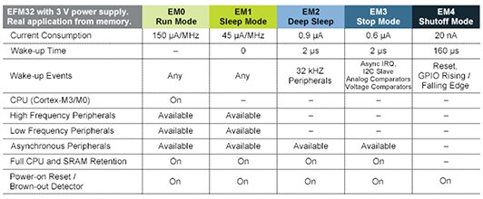
An energy management unit is used to control the different peripherals and memory blocks, allowing unused blocks to be switched off under CPU control. Five modes in the Tiny Gecko (Figure 3) allow fast, slow and asynchronous peripherals to be shut down to save power, before moving to a sleep mode and a ‘stop’ mode to save even more. A Voltage Supply Comparator is also used to monitor the supply voltage from software to manage the power consumption. An interrupt can be generated when the supply falls below or rises above a programmable threshold. The response time and current consumption can be configured by altering the current supply to the comparator.

Figure 3: Five modes in the Tiny Gecko allow the peripheral power consumption to be optimized in wearable designs.
The SoC also includes a Peripheral Reflex System (PRS) that lets the different peripheral module communicate directly with each other without involving the CPU. Peripheral modules that send out Reflex signals are called producers and the PRS matrix routes these reflex signals to the peripherals depending on the data received. This helps reduce the power consumption by reducing the load on the central CPU, allowing it to handle other tasks and shut down if not needed.
Sensors
One of the key applications for wearable designs is the integration and management of a range of sensors. Whether that’s for health monitoring of blood pressure or heart rate, sports performance measurements or proximity sensors for data about the local environment, the interface to the sensors is increasingly important. The Tiny Gecko adds Low Energy Sensor Interface (LESENSE) peripherals that are a highly configurable sensor interface with support for up to eight individually configurable sensors. By controlling the analog comparators and DAC, LESENSE is capable of supporting a wide range of sensors and measurement schemes and can, for instance, measure LC sensors, resistive sensors and capacitive sensors.
LESENSE also includes a programmable FSM that enables simple processing of measurement results without the need for CPU intervention, saving power and allowing the CPU to concentrate on other activities. LESENSE is available in energy mode EM2, in addition to EM0 and EM1, making it ideal for sensor monitoring in applications with a strict energy budget such as a wearable design.
If the designer wants to be more specific about the use of peripherals, there is a range of blocks that can be used to interface to sensors of all kinds. A Successive Approximation Register (SAR) analog-to-digital converter has a resolution of up to 12 bits at up to one million samples per second for taking data from multiple analog sensors, as the integrated input multiplexer can select inputs from eight external pins and six internal signals.
For delivering data output, the 12-bit Digital-to-Analog Converter (DAC) can convert a digital value to an analog output voltage for stimulating sensors or controlling external peripherals such as a small speaker. This has one single ended output buffer connected to channel 0.
If the current output is insufficient, the EFM32TG842 also has three Operational Amplifiers (OPAMPs). These have rail-to-rail differential input and rail-to-rail single ended output, and the input can be set to a pin, the DAC or another OPAMP. The output can be to a pin, another OPAMP or to the ADC. The current is programmable and the OPAMP has various internal configurations such as unity gain or programmable gain using internal resistors.
Graphics
Graphics is an increasingly important element for wearable designs. While there is a debate on the best way to control such systems, from voice to capacitive touchscreens, display technology has been reducing in power and cost to enable new ways of controlling the interface.
For example the Tiny Gecko integrates an LCD driver capable of driving a segmented LCD display with up to 8x18 segments. A voltage boost function enables it to provide the LCD display with higher voltage than the supply voltage for the device. In addition, an animation feature can run custom animations on the LCD display without any CPU intervention. The LCD driver can also remain active even in Energy Mode 2 and provides a Frame Counter interrupt that can wake-up the device on a regular basis for updating data.
Now the new Android Wear operating system is supporting a wider range of displays and this impacts the choice of peripherals in the microcontroller to support higher resolution displays. The memory requirements of the screen and the refresh rate all impact on the size, cost and power consumption of the wearable design. These issues can be handled with a separate graphics processor but this adds complexity, cost and power to the design, and so much of the screen control is integrated into the SoC at the heart of the design.
The ability to support low power, monochrome e-lnk displays is evolving into the need for multiple colors and higher frame refresh rates for wearable designs, especially watches.
For example, Imagination Technologies has developed a new PowerVR graphics processor IP core that provides the industry’s smallest Android compatible GPU graphics solution. With a footprint of just 0.55 mm² and running at 250 MHz in 28 nm silicon, the PowerVR Series5XE GX5300 core features full OpenGL ES 2.0 capability, ultra-low power consumption, and Imagination’s advanced PVRTC texture compression technology. While Imagination is driving the MIPS eco-system around new cores such as microAptiv, the PowerVR GPUS can be used with other processor cores as well.
The new GX5300 core builds upon previous Series5 devices, with substantial improvements in efficiency, providing a low-power solution for entry-level wearable devices and other small footprint embedded applications. The GX5300 uses the PowerVR programmable shader-based tile based deferred rendering (TBDR) architecture that leads to high performance efficiency and the lowest power consumption per frame. Coupled with the PVRTC texture compression technology with the minimum memory footprint for higher image quality, the memory requirements of the display can be significantly reduced.
Imagination provides developers with free access to the PowerVR Graphics SDK, a cross-platform toolkit designed to support all aspects of 3D graphics application development.
General Purpose Input/Output (GPIO)
Not all the peripherals for even a wearable design can be included in the chip, so the general-purpose I/O pins (GPIO) are important. This interface to the outside world is also a key consumer of power, so being able to control these pins carefully is important. As an example, Tiny Gecko has fifty-three GPIO pins divided into ports with up to sixteen pins each. These pins can individually be configured as either an output or input. More advanced configurations like open-drain, filtering and drive strength can also be configured individually for the pins. The GPIO pins can also be overridden by peripheral pin connections, like Timer PWM outputs or USART communication, which can be routed to several locations on the device. The GPIO supports up to sixteen asynchronous external pin interrupts, which enables interrupts from any pin on the device. Also, the input value of a pin can be routed through the Peripheral Reflex System to other peripherals.
Encryption
Increasingly there is a need to keep systems safe and secure, even for wearables. The latest SoC devices add low power encryptions blocks to be used with a wireless link to protect the data that is often sent to the cloud. These blocks support AES encryption and decryption with 128-bit or 256-bit keys, which take different amounts of processing cycles and so consume varying amounts of power. The AES module is often a slave to a bus such as AHB, which enables efficient access to the 32-bit data and key registers.
Conclusion
Wearable designs represent the leading edge of system-on-chip design, with the most peripherals integrated into a single piece of silicon to reduce size and power consumption. The choice and management of these peripherals, both directly and through the latest 32-bit operating systems, makes a significant difference to the overall performance of the end design, particularly in battery life.
免责声明:各个作者和/或论坛参与者在本网站发表的观点、看法和意见不代表 DigiKey 的观点、看法和意见,也不代表 DigiKey 官方政策。


