Introduction to FPGA Part 6 - Verilog Modules and Parameters
2021-12-13 | By ShawnHymel
License: Attribution
A field-programmable gate array (FPGA) is a reconfigurable integrated circuit (IC) that lets you implement a wide range of custom digital circuits. Throughout the series, we will examine how an FPGA works as well as demonstrate the basic building blocks of implementing digital circuits using the Verilog hardware description language (HDL).
Like functions or classes in many programming languages, Verilog offers a way to create modular designs so that you don’t need to copy-and-paste your code. As a result, you can create hierarchical designs to make your code reusable and easier to understand.
In the previous tutorial, we created finite state machines to model hardware that moves sequentially through time as a result of changing inputs. In this guide, we look at creating hierarchical designs using Verilog modules and parameters.
Video
If you have not done so, please watch the following video, which explains the concepts required to complete the challenge. It also demonstrates a working version of the challenge:
Required Hardware
For this challenge, you will need the following hardware:
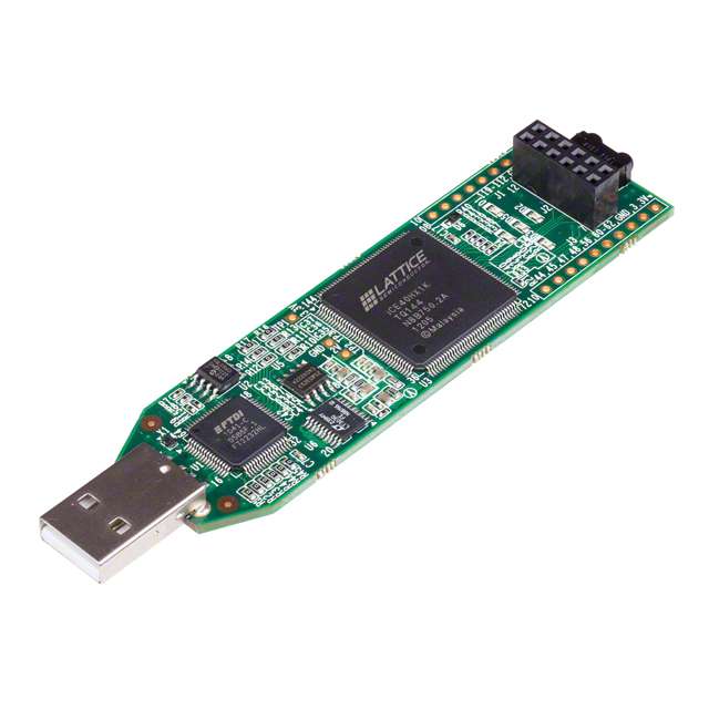
FPGA development board based on the Lattice iCE40. I recommend the iCEstick for this series. However, any of the development boards listed as “supported” by the apio project should work.
(Optional) USB extension cable
Hardware Connections
The PMOD connector at the end of the iCEstick has the following pinout:
A full pinout of the iCEstick can be found here.
Connect 4 pushbuttons to the iCEstick as follows. Note that you do not need pull-up resistors on the buttons. We will use the internal pull-up resistors available in the FPGA.
Resources
The following datasheets and guides might be helpful as you tackle the challenges:
GitHub repository - contains all examples and solutions for this series
Challenge
Your challenge is to create a design that counts up on the LEDs from 0x0 to 0xF and then back down again from 0xF to 0x0. The design should repeat endlessly, counting up and down forever. Additionally, the counter should be slow enough that you can see the individual counts with your eyes, meaning a single count should occur every 0.5 to 1.0 seconds.
You should create this design using modules. I recommend starting with the clock divider module we created in the video. The code for that module can be found here.
Additionally, you will likely want to use a finite state machine (FSM) as the basis for your counter module. You’re welcome to use either Moore-type or Mealy-type state machines as a starting point.
Finally, you will want a top-level design to tie all of these modules together to run your up-and-down counter.
Solution
Spoilers below! I highly encourage you to try the challenge on your own before comparing your answer to mine. Note that my solution may not be the only way to solve the challenge.
Here is how I designed my particular up-and-down counter:
Things are getting a little more complicated! We have to add a good amount of glue logic in our top-level design to make everything work.
To start, we instantiate a clock-divider module so that the clock signal that drives our counters (and other glue logic) is 1 or 2 Hz (slow enough that we can see the counters changing values on the LEDs) rather than 12 MHz.
We then instantiate two different counters. We’ll add parameters to our module code so that we can set the instantiated counter to count up or count down. Notice that the done line from one counter feeds into the go input on the other counter. This is how one counter triggers the next counter to start.
We also need to register a simple initial go pulse to one of the counters. The input to this always block will be the reset line so that when a reset signal is seen, a simple pulse will start the whole counting sequence. We use an OR gate to allow either the done signal from the down counter or the initial go pulse to start the up counter.
Finally, we use a multiplexer (mux) to switch which counter has control of the output LEDs. We need to remember if we’re counting up or counting down, so we create some simple glue logic that toggles the mux control line depending on which done signal is seen from the counter modules.
Rather than paste all of the code in this tutorial, you can find the Verilog for the different modules here:
Paste these files into a new project directory. Navigate to the directory in a terminal. Initialize your project, build it, and upload to the iCEstick:
apio init -b icestick
apio verify
apio build
apio upload
Once the uploading process is complete, you should be able to press the RESET button to start the counting process.
Recommended Reading
The following content might be helpful if you would like to dig deeper:
Introduction to FPGA Part 4 - Clocks and Procedural Assignments
Introduction to FPGA Part 7 - Verilog Testbenches and Simulation
Introduction to FPGA Part 9 - Phase-Locked Loop (PLL) and Glitches


