


制造商零件编号 ICE40HX1K-STICK-EVN
BOARD EVAL FPGA ICESTICK
Lattice Semiconductor Corporation
License: Attribution
Verilog is a hardware description language (HDL), which is a type of computer language used to describe the structure and behavior of electrical circuits (usually digital circuits). In this series, we will use Verilog, as it is supported by the yosys synthesis tool.
Previously, we used continuous assignment statements to construct basic digital logic circuits, including a full 1-bit adder.
In this tutorial, we present one possible solution to creating a clock divider in an FPGA using procedural assignment statements.
Video
If you have not done so, please watch the following video, which explains the concepts required to complete the challenge. It also demonstrates a working version of the challenge:
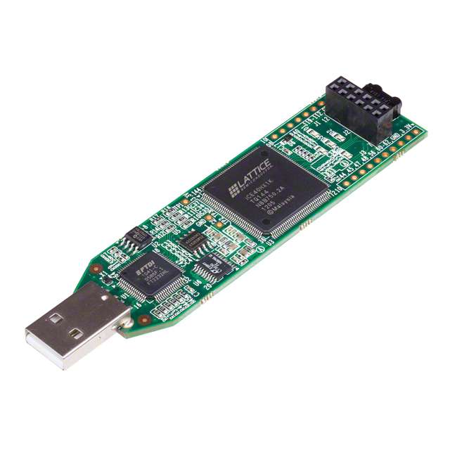
Required Hardware
For this challenge, you will need the following hardware:
Hardware Connections
The PMOD connector at the end of the iCEstick has the following pinout:
A full pinout of the iCEstick can be found here.
Connect 4 pushbuttons to the iCEstick as follows. Note that you do not need pull-up resistors on the buttons. We will use the internal pull-up resistors available in the FPGA.
Resources
The following datasheets and guides might be helpful as you tackle the challenges:
Challenge
Create a clock divider using a counter so that the LEDs count up (in binary) once per second.
The iCEstick has a 12 MHz oscillator connected to physical pin 21 on the FPGA. As a result, you can use the following line in your .pcf file to have a 12 MHz clock signal on the “clk” input in Verilog:
set_io clk 21
Hint: you will probably need two counters in your design--one to operate as a clock divider and another to count up on the LEDs.
Solution
Spoilers below! I highly encourage you to try the challenge on your own before comparing your answer to mine. Note that my solution may not be the only way to solve the challenge.
[Edit 12/28/2021] IMPORTANT: the solution below is a useful clock divider design for beginners, but it can lead to errors down the road when we talk about metastability. For a better clock divider that does not rely on an asynchronous clock signal, please see here.
clock-counter.pcf
# Oscillator
set_io              clk     21

# LEDs
set_io              led[0]  99
set_io              led[1]  98
set_io              led[2]  97
set_io              led[3]  96

# PMOD I/O
set_io  -pullup yes rst_btn 78
clock-counter.v
// Clock-divided counter
//
// Inputs:
//      clk         - 12 MHz clock
//      rst_btn     - pushbutton (RESET)
//
// Outputs:
//      led[3:0]    - LEDs (count from 0x0 to 0xf)
//
// LEDs will display a binary number that increments by one each second.
//
// Date: October 26, 2021
// Author: Shawn Hymel
// License: 0BSD

// Count up each second
module clock_counter (

    // Inputs
    input               clk,
    input               rst_btn,

    // Outputs
    output  reg [3:0]   led
);

    wire rst;
    reg div_clk;
    reg [31:0] count;
    localparam [31:0] max_count = 6000000;

    // Reset is the inverse of the reset button
    assign rst = ~rst_btn;

    // Count up on (divided) clock rising edge or reset on button push
    always @ (posedge div_clk or posedge rst) begin
        if (rst == 1'b1) begin
            led <= 4'b0;
        end else begin
            led <= led + 1'b1;
        end
    end

    // Clock divider
    always @ (posedge clk or posedge rst) begin
        if (rst == 1'b1) begin
            count <= 32'b0;
        end else if (count == max_count) begin
            count <= 32'b0;
            div_clk <= ~div_clk;
        end else begin
            count <= count + 1;
        end
    end

endmodule
Save these files in a single directory on your computer. Open a terminal and enter the following apio commands to initialize the board (assuming you are using an iCEstick), build the project, and upload it to your FPGA development board:
apio init -b icestick
apio build
apio upload
When the process is done, the LEDs should count up (in binary) once per second. Press the first pushbutton to reset the counter.
Explanation
The .pcf file should be very similar to what you used in the previous challenge. The big difference is the addition of the clock signal. The 12 MHz is permanently attached to physical pin 21 on the FPGA, and we assign the name “clk” to that signal.
After defining our input and output signals, we declare our local wires, registers, and parameters:
    wire rst;
    reg div_clk;
    reg [31:0] count;
    localparam [31:0] max_count = 6000000;
Note that we introduce a new declaration here: the parameter. Parameters are used to hold constant values during runtime (e.g. numbers used for calculations). You can change a parameter’s value at synthesis time if you are instantiating a module in another module (see this article for more detail: https://www.chipverify.com/verilog/verilog-parameters).
In our case, we are using a “localparam,” which sets a constant numerical value in our module and prevents it from being overridden by a “defparam” or argument call from a top-level module. See this discussion for more information: https://stackoverflow.com/questions/30288783/difference-between-parameter-and-localparam.
Note that we must set the number of bits required to hold this value. In this example, we need 32 bits (given by [31:0]) to hold the value 6000000.
Next, we use a continuous assignment to invert the reset button signal (so that it can trigger a reset on a rising edge). Alternatively, you could could use “negegde” in the sensitivity list for the reset button if you did not want to invert the signal. The counter is implemented in the always block, which defines a set of procedural assignments.
    // Count up on (divided) clock rising edge or reset on button push
    always @ (posedge div_clk or posedge rst) begin
        if (rst == 1'b1) begin
            led <= 4'b0;
        end else begin
            led <= led + 1'b1;
        end
    end
Next, we need to create the actual clock divider, which converts the 12 MHz clk signal to a 1 Hz signal (named “clk_div”).
The clock divider is just another counter block. Just like the first counter block, the counter signal resets to 0 if the reset button is pressed. Next, if the counter reaches the maximum value (6,000,000) as set by the max_count localparam, it resets back to 0 and the div_clk signal toggles. Finally, if neither of those conditions are met, the count value increments by one.
    // Clock divider
    always @ (posedge clk or posedge rst) begin
        if (rst == 1'b1) begin
            count <= 32'b0;
        end else if (count == max_count) begin
            count <= 32'b0;
            div_clk <= ~div_clk;
        end else begin
            count <= count + 1;
        end
    end
We count to 6,000,000 twice to make one complete cycle (low and high) for the div_clk signal. That’s how we convert 12 MHz to 1 Hz!
Recommended Reading
The following content might be helpful if you would like to dig deeper:
Introduction to FPGA Part 1 - What is an FPGA?
Introduction to FPGA Part 2 - Toolchain Setup
Introduction to FPGA Part 3 - Getting Started with Verilog
Introduction to FPGA Part 5 - Finite State Machine (FSM)
Introduction to FPGA Part 6 - Verilog Modules and Parameters
Introduction to FPGA Part 7 - Verilog Testbenches and Simulation
Introduction to FPGA Part 8 - Memory and Block RAM
Introduction to FPGA Part 9 - Phase-Locked Loop (PLL) and Glitches
Introduction to FPGA Part 10 - Metastability and FIFO
Introduction to FPGA Part 11 - RISC-V Softcore Processor
Introduction to FPGA Part 12 - RISC-V Custom Peripheral

