Introduction to FPGA Part 12 - RISC-V Custom Peripheral
2022-01-31 | By ShawnHymel
License: Attribution RISC-V
A field-programmable gate array (FPGA) is a reconfigurable integrated circuit (IC) that lets you implement a wide range of custom digital circuits. Throughout the series, we will examine how an FPGA works as well as demonstrate the basic building blocks of implementing digital circuits using the Verilog hardware description language (HDL).
RISC-V is an open-source instruction set architecture (ISA) that allows anyone to implement a central processing unit (CPU) or system-on-a-chip (SOC) design without paying a licensing fee. As a result, it is popular with FPGA enthusiasts as the starting point for a softcore processor implementation.
In the previous tutorial, we demonstrated how to implement the FemtoRV SOC on the iCEstick and created a C program to blink the onboard LEDs. You were challenged to modify the Verilog code to enable the buttons module. This time, we show how to create a custom hardware peripheral in Verilog and integrate it into the RISC-V softcore processor.
Video
This tutorial can also be viewed in video form:
Required Hardware
For this tutorial, you will need the following hardware:
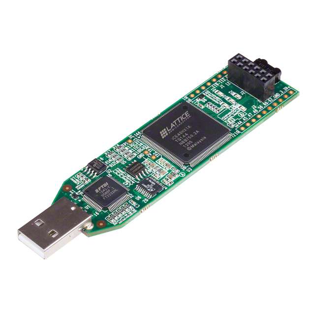
FPGA development board based on the Lattice iCE40. I recommend the iCEstick for this series. However, any of the development boards listed as “supported” for the FemtoRV SOC should work.
(Optional) USB extension cable
Hardware Connections
The PMOD connector at the end of the iCEstick has the following pinout:
A full pinout of the iCEstick can be found here.
Connect 4 pushbuttons to the iCEstick as follows. Note that you do not need pull-up resistors on the buttons. We will use the internal pull-up resistors available in the FPGA.
Resources
The following datasheets and guides might be helpful as you tackle the challenges:
GitHub repository - contains all examples and solutions for this series
learn-fpga GitHub repository - contains Bruno Levy’s RISC-V implementation (FemtoRV)
PWM Peripheral
We will create a simple pulse-width modulation (PWM) peripheral. The SOC can write a value to the peripheral’s register. The PWM module will maintain a counter that continuously counts (e.g. up to 4095, resets to 0, and then back to 4095 over and over). Whenever the counter is less than the PWM register value, the output line (e.g. pin) will be high. Whenever it is greater than or equal to the register value, the output line will be low. This creates the following pattern:
So long as our clock speed is fast enough, the PWM (if driving an LED) should appear steady to our eyes.
On your host computer, head to the learn-fpga repository and create the PWM driver:
cd ~/Projects/fpga/learn-fpga/FemtoRV
nano RTL/DEVICES/pwm.v
In that file, enter the following Verilog code. If you’ve been following along with the series, this code should be straightforward to decipher.
// Control brightness of one of the LEDs
module pwm #(

    // Parameters
    parameter       WIDTH = 12  // Default PWM values 0..4095

) (

    // Inputs
    input           clk,
    input           wstrb,  // Write strobe
    input           sel,    // Select (read/write ignored if low)
    input   [31:0]  wdata,  // Data to be written (to driver)

    // Outputs
    output  [3:0]   led
);

    // Internal storage elements
    reg             pwm_led = 1'b0;
    reg [WIDTH-1:0] pwm_count = 0;
    reg [WIDTH-1:0] count = 0;

    // Only control the first LED
    assign led[0] = pwm_led;

    // Update PWM duty cycle
    always @ (posedge clk) begin

        // If sel is high, record duty cycle count on strobe
        if (sel && wstrb) begin
            pwm_count <= wdata[WIDTH-1:0];
            count <= 0;

        // Otherwise, continuously count and flash LED as necessary
        end else begin
            count <= count   1;
            if (count < pwm_count) begin
                pwm_led <= 1'b1;
            end else begin
                pwm_led <= 1'b0;
            end
        end
    end

endmodule
Save and exit. You are welcome to simulate the PWM design with a separate testbench. You can find my PWM code and testbench here.
Memory Addressing
To communicate with peripherals, FemtoRV relies on a unique memory addressing scheme. Memory addresses are 32 bits. However, bits 24..31 and bits 0..1 are not used. Bits 22..23 are used to access different “pages.”
A page is where we want to read or write data. For example, if bits 22...23 are ‘b00, then we can access physical RAM (implemented as block RAM in the iCEstick). We have 20 bits of addresses we can use to communicate with block RAM (bits 2..21). That means addresses 0x00000000..0x003FFFFC (in CPU instructions) are used to read/write to RAM.
However, only the first 6 kB of that space is actually available to us as physical RAM. The iCE40-HX1K has 8 kB of block RAM, and 2 kB are set aside for general purpose registers.
If bits 22..23 are ‘b01, then it means we want to access a special purpose register (e.g. a register in one of our hardware peripherals).
If bits 22..23 are ‘b10, then it means we want to access program memory, which is stored in the SPI flash chip on the iCEstick.
For the special purpose registers (in “I/O memory address space”), peripheral addresses are given by a one-hot encoding scheme. A one-hot scheme means that only one bit is high at a time for each address. There are 20 bits of address space available (bits 2..21), so there are 20 total addresses for us to use for hardware peripherals.
If you look in the HardwareConfig_bits.v file, you can see that bits 0..11 are taken up by existing hardware peripherals, and bits 17..19 are reserved for constant hardware registers (e.g. CPU information). We will need to modify this file (along with some others) to integrate our PWM driver.
Modify FemtoRV
To integrate this peripheral into the FemtoRV design, we need to make a few changes to the original Verilog code. Start by adding a PWM device bit number to the HardwareConfig_bits.v file:
nano RTL/Devices/HardwareConfig_bits.v
Add the following line just after “localparam IO_FGA_DAT_bit = 11;”
localparam IO_PWM_bit = 12; // W write duty cycle (12 bits)
Save and exit. Modify the top-level femtosoc.v file:
nano RTL/femtosoc.v
Make the following changes to the Verilog code:
...

`include "DEVICES/FGA.v"            // Femto Graphic Adapter
`include "DEVICES/HardwareConfig.v" // Constant registers to query hardware con$
`include "DEVICES/pwm.v"            // PWM driver for one LED

...

module femtosoc(
`ifdef NRV_IO_LEDS
 `ifdef FOMU
   output rgb0,rgb1,rgb2,
 `else
   output D1,D2,D3,D4,D5,
 `endif
`endif
`ifdef NRV_IO_PWM
  output D1,D2,D3,D4,D5,
`endif

...

/****************************************************************/
/* PWM Peripheral                                               */
`ifdef NRV_IO_PWM
  pwm #(
    .WIDTH(12)
  ) pwm (
    .clk(clk),
    .wstrb(io_wstrb),
    .sel(io_word_address[IO_PWM_bit]),
    .wdata(io_wdata),
    .led({D4, D3, D2, D1})
  );
`endif

/****************************************************************/
/* And last but not least, the processor                        */

...
Save and exit. In the iCEstick hardware configuration file, we need to disable the LEDs so we can have the PWM module control one of the LEDs.
nano RTL/CONFIGS/icestick_config.v
Change the Devices section to look like the following:
`define NRV_IO_BUTTONS       // Mapped IO to PMOD connector (78, 79, 80, 81)
//`define NRV_IO_LEDS          // Mapped IO, LEDs D1,D2,D3,D4 (D5 is used to di$
//`define NRV_IO_IRDA          // In IO_LEDS, support for the IRDA on the IceSt$
`define NRV_IO_UART          // Mapped IO, virtual UART (USB)
//`define NRV_IO_SSD1351       // Mapped IO, 128x128x64K OLED screen
//`define NRV_IO_MAX7219       // Mapped IO, 8x8 led matrix
`define NRV_MAPPED_SPI_FLASH // SPI flash mapped in address space. Use with MIN$
`define NRV_IO_PWM           // Use PWM peripheral to control LED
Save and exit. Build and upload the new SOC design:
make ICESTICK
Example Software
Note that we did not update FIRMWARE/LIBFEMTORV32/femtorv32.h to include the memory addressing macros. You’re welcome to add those macros, but I’m going to manually address the I/O memory space to talk directly to the PWM hardware.
cd ~/Projects/fpga
mkdir -p femtorv32/pwm_test
cd femtorv32/pwm_test
nano main.c
Here is a simple C program that ramps up the brightness of the LED connected to the PWM peripheral, resets it to 0 (off), and repeats the process.
#include <femtorv32.h>

int main() {
    while (1) {
        for (int i = 0; i < 4096; i  ) {
            *(volatile uint32_t*)(0x404000) = i;
            delay(1);
        }
    }
}
Save and exit. Create a Makefile that includes the FemtoRV Makefile template.
nano Makefile
Add the following line:
include ../../learn-fpga/FemtoRV/FIRMWARE/makefile.inc
Save and exit. Build and upload the software:
make main.prog
The first LED on the iCEstick should slowly increase in brightness over time, reset to off, and continue the process. It will take a little over 4 seconds to complete one cycle.
There is no real challenge for this final episode. If you made it this far, feel free to celebrate! You should have many of the basic building blocks to start creating your own FPGA designs and working within larger Verilog projects.
If you’d like an open-ended challenge, try designing your own, custom hardware peripheral for the FemtoRV. Share your project on Twitter and tag us if you make something cool (@DigiKey, @MakerIO, @ShawnHymel, @BrunoLevy01, #FemtoRV).
Recommended Reading
The following content might be helpful if you would like to dig deeper:
Introduction to FPGA Part 4 - Clocks and Procedural Assignments
Introduction to FPGA Part 6 - Verilog Modules and Parameters
Introduction to FPGA Part 7 - Verilog Testbenches and Simulation
Introduction to FPGA Part 9 - Phase-Locked Loop (PLL) and Glitches


