


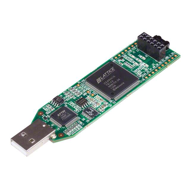
制造商零件编号 ICE40HX1K-STICK-EVN
BOARD EVAL FPGA ICESTICK
Lattice Semiconductor Corporation
License: Attribution
A field-programmable gate array (FPGA) is a reconfigurable integrated circuit (IC) that lets you implement a wide range of custom digital circuits. These custom digital circuits can be used to create optimized circuits for things like digital signal processing (DSP), machine learning, and cryptocurrency mining. They are found in many consumer electronics as well as on specialized equipment, such as satellites and communication equipment.
Throughout the series, we will examine how an FPGA works as well as demonstrate the basic building blocks of implementing digital circuits using the Verilog hardware description language (HDL). You will have the opportunity to synthesize and upload your code to a real FPGA.
In this first part, we will look at why you might want to choose an FPGA over other solutions (e.g. microcontrollers) as well as give some examples of where FPGAs are commonly used.
See here if you would like to view this part in video format:
Required Hardware
For this series, you will need the following hardware:
If other hardware is needed for a particular episode, it will be listed in the video as well as in the written tutorial.
Reconfigurable Hardware
An FPGA provides a way to implement custom digital logic circuits in a short amount of time using an HDL. Prior to reconfigurable logic ICs, engineers would have to wire up breadboards to test their ideas.
Image credits: “breadboard - 1” by Windell Oskay is licensed under CC BY 2.0.
As you can imagine, complex digital designs would create wiring nightmares, and tracking down bugs became nearly impossible. Reconfigurable logic ICs (e.g. CPLDs and FPGAs) offer a way to reduce space, wiring clutter, and debugging effort.
An FPGA is made of many Programmable Logic Blocks (PLBs), each of which contains several Logic Cells. In the FPGA used in the series (the Lattice iCE40HX1K on the iCEstick), each PLB contains 8 cells. This number may change depending on your particular FPGA.
The following diagram (taken from the iCE40LP/HX datasheet) shows the different parts of the iCE40LP/HX FPGA.
Each cell contains a D flip-flop and a Lookup Table (LUT). We will explore these components in future episodes.
In addition to these blocks, most FPGAs will contain some random access memory (RAM) for short-term storage of data, a phase-locked loop (PLL) to act as a clock multiplier, and some input/output (I/O) banks that allow you to use the various pins as digital inputs or outputs. Some offer additional peripherals, such as dedicated communication blocks (e.g. SPI), analog-to-digital converters (ADCs), or even on-chip central processing units (CPUs) for running sequential code.
When you “program” an FPGA, you tell it how to connect these various blocks and peripherals together to implement your digital circuit!
What Is It Good For?
Making designs for an FPGA is an intermediate or advanced engineering topic, as you need to have a fundamental understanding of digital circuits, which includes logic gates, binary, and boolean algebra.
Important! This series assumes you have some basic knowledge of digital circuits. We will focus on implementing these designs in an HDL, testing them through simulation, and uploading them to an FPGA.
In many cases, you will often find that a microcontroller or microprocessor (e.g. single board computer) can get the job done for less effort. However, there are a number of applications where you need to have reconfigurable digital logic. Let’s look at a few examples:
Because you can reconfigure it in the field, the FPGA makes for a fantastic prototyping tool. You can tweak and refine your digital circuit until it meets your requirements. If you plan to produce more than a few thousand units of your final product, you might consider turning your custom digital circuit into an application-specific integrated circuit (ASIC). With an ASIC, your digital circuit design is permanently etched into an integrated circuit (“chip”) that you can include in your product. However, the tooling costs for an ASIC might be prohibitive.
If you plan to produce less than a few thousand units of your product, you might consider just adding the FPGA to your design, as Mercedes-Benz did in one of their infotainment consoles.
Design Flow
The following diagram shows a typical process for creating a design for an FPGA. If you are used to programming for computers or microcontrollers, you will notice that the naming of the steps are different (e.g. there is no “compile” step) than what you might be used to.
Note that each step lists the tool we plan to use throughout this series.
Don’t worry! You won’t need to install and use these tools individually. We will rely on the open-source and cross-platform tool apio to help manage these tools. As an analogy, if yosys is like avr-gcc, then apio is like the Arduino IDE. Apio is specifically made to work with popular iCE40 development boards, and it makes the building/uploading process much easier so that we can focus on learning the building blocks of FPGA design.
Recommended Reading
All demonstrations and solutions for this series can be found in this GitHub repository.
You can learn more about the apio tool on their documentation site.
Introduction to FPGA Part 2 - Toolchain Setup
Introduction to FPGA Part 3 - Getting Started with Verilog
Introduction to FPGA Part 4 - Clocks and Procedural Assignments
Introduction to FPGA Part 5 - Finite State Machine (FSM)
Introduction to FPGA Part 6 - Verilog Modules and Parameters
Introduction to FPGA Part 7 - Verilog Testbenches and Simulation
Introduction to FPGA Part 8 - Memory and Block RAM
Introduction to FPGA Part 9 - Phase-Locked Loop (PLL) and Glitches
Introduction to FPGA Part 10 - Metastability and FIFO
Introduction to FPGA Part 11 - RISC-V Softcore Processor
Introduction to FPGA Part 12 - RISC-V Custom Peripheral

