Using an Inverting Regulator for Buck/Boost DC-to-DC Voltage Conversion
投稿人:电子产品
2015-08-18
Step-down (“buck”) switching voltage converters (or regulators) are popular for battery-powered products because they are efficient over wide ranges of voltage and load and are relatively simple. However, when the battery voltage drops below the required output, the regulator stops operating. This can be a drawback in portable designs because there is often some unused capacity left in the battery after the power supply “drops out” which could otherwise have been used to extend run time.
A popular solution to address unused battery capacity is the step-down/step-up (“buck/boost”) switching regulator or an alternative topology such as single-ended primary inductor converter (SEPIC). (See the TechZone article “The SEPIC Option for Battery-Power Management”.) These types of power supplies automatically switch to a boost configuration once the battery output falls below the desired power supply output; but buck/boost devices are relatively expensive, the circuitry is more complex, and the power supply takes up greater board space.
However, there is a lesser-known option for a switching power supply which maximizes battery capacity in a portable product yet is simple and inexpensive: the switching inverting regulator. These are usually employed to convert a positive input voltage to a (lower) negative output, but can also be used to convert a varying positive input to a lower or higher negative output.
This article describes the function of a switching inverting regulator and its application and then leads on to describe a topology that uses the device to regulate a varying input voltage as an alternative to a conventional buck/boost regulator.
Anatomy of an inverting regulator
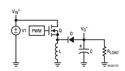
Figure 1 shows a simplified schematic of a switching inverting regulator. The regulator comprises a pulse width modulation (PWM) controller driving a metal oxide semiconductor field effect transistor (MOSFET) connected to an inductor. The inductor acts as an energy reservoir providing power when the storage MOSFET switches off.

Figure 1: Simplified schematic of a switching inverting voltage regulator. (Courtesy of Linear Technology)
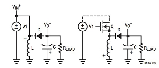
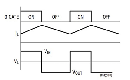
Figures 2(a) and 2(b) show equivalent circuits, illustrating what happens during the operation of the circuit shown in Figure 1. When transistor (Q) is on (Figure 2(a)), diode (D) is reverse biased and the current in the inductor (L) increases. When Q is off (Figure 2(b)), the L changes polarity, D becomes forward biased and current flows from L to the load and capacitor (C). The voltage across C and the load is negative, relative to system ground. Figure 3 shows the timing diagram for the circuit.

Figures 2(a) at left and 2(b): Equivalent circuits illustrating the operation of a switching inverting regulator. (Courtesy of Linear Technology)

Figure 3: Timing diagram for a switching inverting regulator. (Courtesy of Linear Technology)
VMAX is the maximum voltage across Q and D (Figures 2(a) and 2(b)), where:
![]()
The maximum current, IMAX, through Q, L, and D can be derived using the following equations, assuming continuous conduction mode:
![]()
Where t is the switching period1.
Inverters in buck/boost applications
The switching inverting regulator is popular with engineers for applications including double-ended sensors and audio amplifiers, among others. However, today’s generation of high-voltage, synchronous inverting regulators is finding a second application as an alternative to conventional buck/boost, SEPIC, and flyback topologies for buck/boost operation.
The inverting regulator can be used to convert a (sometimes widely) varying positive input to a lower or higher negative output – providing a simpler (typically just using a single inductor) and less expensive alternative to the more established buck/boost power supply designs.
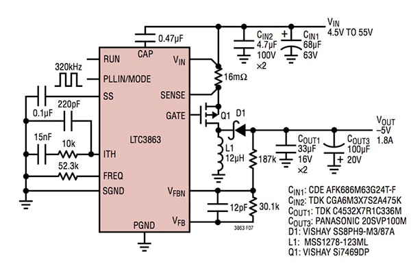
There is a wide choice of DC-to-DC switching controllers upon which an inverting voltage regulator circuit can be based. For example, Figure 4 shows a Linear Technology LTC3863 inverting DC-to-DC controller in a typical buck/boost application. The LTC3863 is optimized for automotive and industrial applications. The chip drives a P-channel power MOSFET to generate a negative output and requires just a single inductor to complete the circuit. Output voltages from –0.4 to –150 V are possible with higher voltages limited only by the rating of external components. The LTC3863 offers excellent light load efficiency, drawing only 70 μA quiescent current. The switching frequency can be programmed from 50 to 850 kHz.
When used as a controller for a P-channel MOSFET plus inductor and diode (and supporting passives), the LTC3863 supports an inverting regulator topology that combines the simplicity of a buck converter with the regulation range of a conventional buck/boost topology. In this configuration, the circuit supplies an output voltage of –5 V at a maximum current of 1.8 A from an input voltage of 4.5 to 55 V (at a switching frequency of 320 kHz).

Figure 4: LTC3863 DC-to-DC switching controller-based inverting power supply example design. (Courtesy of Linear Technology)
The entire converter power path contains the LTC3863, MOSFET Q1, inductor L1, diode D1, and output filter capacitors COUT1 and COUT3.
Texas Instruments’ TPS5430, promoted as a buck controller for conventional power supply topologies, can also be configured as the basis of an inverting buck/boost design. This chip integrates the MOSFET switching element. Operating frequency is 500 kHz and the device accepts a wide input voltage range of -0.3 to 40 V and provides 1.2 to 31 V output at up to 3 A (continuous) or 4 A (peak) current with an efficiency up to 95 percent.
For its part, Maxim offers its MAX765 switching inverting regulator which can be used in buck/boost topologies. The input voltage range of the device is 3 to 16 V and the output voltage is preset at -12 V (but can also be adjusted from -1 V to -16 V using two external resistors). The maximum operating (VIN - VOUT) differential is 20 V.
In summary, the switching inverting regulator can be a simpler and less expensive option for buck/boost operation than a conventional buck/boost device. The downside of using a switching-inverting regulator in this type of application is that the output voltage is negative. However, reversing the polarity of the circuit is straightforward; the circuit can be designed such that the negative output is set as the system ground with the negative battery terminal then becoming the “positive” voltage source. The effective voltage across the input of the device will be VIN – VOUT2.
For more information about the parts discussed in this article, use the links provided to access product pages on the DigiKey website.
References:
- “A Positive-to-Negative Voltage Converter Can Be Used for Stable Outputs Even with a Widely Varying Input,” Victor Khasiev, Linear Technology Design Note 433, 2008.
- “Using the TPS5430 as an Inverting Buck-Boost Converter,” John Tucker, Texas Instruments Application Report, August 2007.
免责声明:各个作者和/或论坛参与者在本网站发表的观点、看法和意见不代表 DigiKey 的观点、看法和意见,也不代表 DigiKey 官方政策。


 中国
中国