Using PFM to Improve Switching DC/DC Regulator Efficiency at Low Loads
投稿人:电子产品
2014-02-25
Switching DC/DC voltage converters (“regulators”) are popular because of their high efficiency over a wide voltage input range. The voltage regulation is determined by pulse width modulation (PWM) that rapidly switches the regulator’s internal MOSFET (or MOSFETs in a synchronous device). The technique generally works well, but at low loads efficiency tails off rapidly, which can shorten battery life in portable products, particularly those that spend a lot of time in a “standby” mode.
Silicon vendors use several methods to improve the efficiency of switching regulators under low loads, including soft switching and discontinuous conduction mode. More recently, pulse frequency modulation (PFM), a variation on PWM, has joined this list.
This article takes a close look at PFM and compares how the technique improves efficiency at low power compared with a device that uses PWM across the entire load range.
PWM voltage regulator control
A simple and inexpensive way to regulate battery voltage in a portable electronic device is to use a linear regulator or low-dropout regulator (LDO). Unfortunately, when the input voltage is much higher than the output, efficiency is poor and power is dissipated as heat (see the TechZone article “Understanding the Advantages and Disadvantages of Linear Regulators”). Higher efficiency, at the expense of cost and component size, is achieved using a switching regulator that combines rapidly-switching MOSFETs and energy storage in an inductor’s magnetic field.
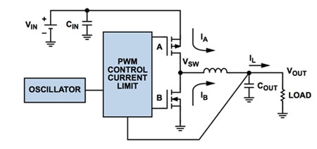
In contemporary “low-low power” switching regulators, PWM is the primary operating mode. Figure 1 shows a synchronous step-down (“buck”) converter using PWM control.

Figure 1: A synchronous buck voltage regulator with PWM control (Courtesy of Analog Devices).
The oscillator and PWM controller produce a rectangular pulse wave that switches the MOSFETs of the switching regulator at a set frequency, typically in the hundreds of megahertz range. The output voltage of the regulator is proportional to the duty cycle (“D”) from the formula:
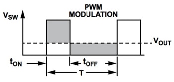
D = tON / (tON + tOFF) ≈ VOUT/VIN
Figure 2 shows this graphically.

Figure 2: The output voltage of the regulator is proportional to the duty cycle (Courtesy of Analog Devices).
A voltage- or current-feedback control loop alters the PWM controller output to regulate the output voltage in response to load changes.¹
Unfortunately, the efficiency of a switching regulator tails off at lower loads. Under these loads, power losses result from current ripple-induced conduction losses, and so-called “V–I overlap” switching losses associated with the voltage-current, overlap common to a rapid switching cycle. V-I overlap losses are proportional to load current, input voltage, and switching frequency.
The conduction losses caused by the current ripple become dominant because the overlap loss scales down with the load current, while the power dissipated by current ripple normally remains constant. When the voltage regulator is under very-light load, the gate-drive losses, consumed when charging and discharging the gate capacitances of the power transistors during switching transitions, dominate (see the TechZone article “Techniques to Limit Switching DC/DC Converter Inefficiency During Low Loads”).
Silicon vendors use a number of techniques to address these losses and increase the efficiency of switching regulators under low loads. For example, “soft switching” eliminates overlap losses by switching the power transistor when either its voltage or its current is zero. Another technique is to allow the switching regulator to idle by skipping pulses in the pulse train.
Analog Devices implements a pulse-skipping mode when its ADP2108 voltage regulator is under low-load conditions using a pulse-skipping technique. The chip is a 3 MHz buck regulator offering 3.3 V output from 2.3 to 5.5 V input at up to 600 mA.
During the power-saving mode, an offset induced in the PWM regulation level causes the output voltage of the ADP2108 to increase until it reaches approximately 1.5 percent above the PWM regulation level, at which point PWM operation turns off and both MOSFETS are idle. When the output voltage falls below the PWM regulation voltage, switching restarts, causing the output voltage rise to the upper threshold. This process is repeated as long as the load current is below the power-saving current threshold. The device offers 85 percent efficiency (VIN = 2.7 V, VOUT = 1.8 V) at 2 mA output current.
Improving efficiency with PFM
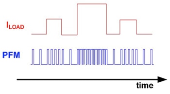
An increasingly popular efficiency-enhancing technique is PFM. PFM control is similar to PWM control in that it employs a rectangular pulse train to determine the output voltage of the regulator. However, instead of altering the duty cycle of the pulse train of a fixed frequency to set the output voltage, PFM alters the frequency of a pulse train of fixed duty cycle.
During PFM operation, the output power is proportional to the average frequency of the pulse train. The converter only operates when the output voltage drops below the set output voltage as measured by the feedback control loop. The frequency of converter switching is then increased until the output voltage reaches a typical value between the set output voltage and 0.8 to 1.5 percent above the set output voltage.
Figure 3 illustrates the technique which some manufacturers refer to as “power-saving mode.”

Figure 3: PFM varies the frequency of a rectangular pulse train of fixed duty cycle to meet load demand.
The advantage of PFM is significantly-improved efficiency under low loads because there are periods where the MOSFETs switch slowly or not at all, reducing switching losses. In some devices, when pulses are skipped, the regulator is completely powered down, further reducing the chip’s quiescent current and enhancing efficiency.²
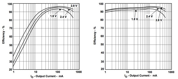
Figures 4(a) and (b) show how PFM improves the efficiency of Texas Instruments’ (TI) TPS61020 compared with PWM control. The TI voltage regulator is a step-up (“boost”) device that runs at 600 kHz in PWM mode and provides a 1.8 to 5.5 V output from a 0.9 to 6.5 V input. Maximum output current is 1.5 A.

Figure 4a and b: Efficiency of TI TPS61020 in PWM mode (left) compared with efficiency in “power save” (PWM plus PFM at low loads) mode.
Maxim’s MAX8632 also takes advantage of PFM. The component uses a comparator to sense when the current through the inductor reverses and opens the switch, allowing the MOSFET’s body diode to block the reverse current, bringing the voltage across the inductor to zero. A new cycle is then initiated when the output voltage drops below the regulating threshold. Switching frequency is proportional to the load current.
PFM operation is not limited to low-voltage regulators. Maxim’s MAX17503 buck regulator is a high-voltage device capable of accepting an input from 4.5 to 60 V to deliver a 0.9 to 54 V output at up to 2.5 A. The MAX17503 features a PFM mode that boosts efficiency to 75 percent when the device is delivering 5 V from a 24 V input at a load current of just 6 mA.
There are some drawbacks to PFM, including increased voltage ripple at the output that can cause electromagnetic interference (EMI) problems in sensitive circuits adjacent to the regulator (see the TechZone article “Hybrid Power Supplies Deliver Noise-Free Voltages for Sensitive Circuitry”). This is the key reason why PWM is generally preferred for switching control at the higher loads where efficiency is less compromised by the technique. A second drawback to PFM is a lack of response of the regulator to rapid changes in load.
PWM will remain the workhorse for precise control of switching regulators under most load conditions. However, modern products that combine PWM with a power-saving PFM mode when operating under low loads are a good solution for a design engineer striving to maximize the battery life of his or her portable product.
References:
- “How to Apply DC-to-DC Step-Down (Buck) Regulators Successfully,” Ken Marasco, Analog Devices, Analog Dialogue 45-06 Back Burner, June 2011.
- “PWM and PFM Operation of DC/DC Converters for Portable Applications,” Upal Sengupta, Texas Instruments.
免责声明:各个作者和/或论坛参与者在本网站发表的观点、看法和意见不代表 DigiKey 的观点、看法和意见,也不代表 DigiKey 官方政策。


