Power Regulation Constrains Design
投稿人:Convergence Promotions LLC
2012-11-13
The portable and embedded product spaces have moved on from simpler days where the entire system infrastructure was based on 12 V analog sensors and 5 V logic levels. With the increased use of embedded displays, new sensors, memory, I/Os and advanced low-power controllers, most embedded systems now require a large variety of power domains, which may include a mixture of 0.8 to 1.8 V, 2.3 V, 2.7 V, 3.3 V, 5 V and 12 V supplies.
External mains transformers only supply one voltage level, so the rest must be generated on the PCB. This is typically done using a number of different individual power regulators or a single more complex power management IC (PMIC). The selection of these ICs is based on the voltage output, the current levels supported, and the thermal operating conditions of the design.
Why multiple power supplies?
Today's embedded systems are often designed using multiple technologies. Most designs have a combination of components that include MOS, bipolar, MEMS, TFT-LCD, and LED technologies. As process and manufacturing scaling has progressed, the nominal operative voltage for ICs has dropped. The amount of current per transistor has also dropped; however, since there are more transistors per chip in most designs, the net current draw has not necessarily gone down. The use of mixed technology in a design is driving the need for multiple power regulators.
A second driver for multiple supplies is power reduction. New designs segment the power domains by function, and applications need to be able to quickly switch the power for those segments on and off. To optimally reduce power for individual blocks, it is best to give them stand-alone, high-level power-gating control and regulation. This results in a design with multiple local power regulators that are connected to a master power line.
This segmented design flow requires a number of different power regulation technologies. These include, but are not limited to, linear regulators, low drop-out (LDO) regulators, DC-DC converters – including boost, buck and boost-buck regulators – and charge pump circuits.
Linear and LDO regulators
The basic function of LDO regulators is just what the name implies: an input voltage of one level has some variation and produces an output of another level that holds the value more precisely than the input level. Most linear and LDO regulators produce an output voltage that is less than or equal to the input voltage. These regulators utilize an external resistor pair and a hold capacitor to help set and stabilize the output level.
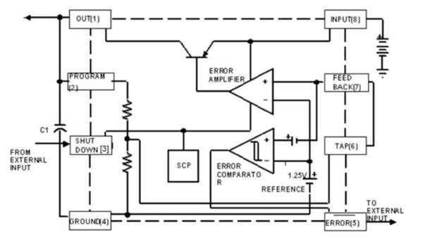
As shown in Figure 1, a typical linear regulator (Fairchild Semiconductor’s LP2951) includes a shut-down control. Linear regulators are generally used for always-on applications. The increased functionality of mobile devices requires that power control be switchable. In the LP2951, the output of the regulator is available when the shutdown signal is low, and when it is over a threshold defined by the input voltage, the output goes to an “off” or high impedance state and does not provide any output current.
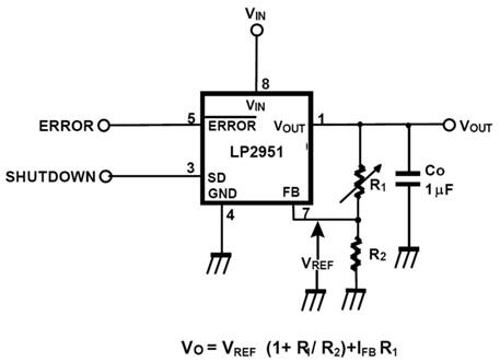
The adjustable voltage outputs are generally selected for memory applications, since the same system and board may incorporate memory from different speed and performance classes. These memory differences dictate requirements for both current draw and operating voltage. Adjustable linear and LDO regulators enable a common bill of materials across different boards, with just a small change in the passive components for different applications.
DC-DC switching buck regulators
Continuing with regulators that produce a lower voltage than the reference supply, we have the active switching DC-DC converters of the buck variety. These use active logic control and timing circuits to enable high efficiency (over 90 percent). Buck regulators, despite being efficient and delivering a stable output, have a high frequency ripple due to the clock and switching noise present in their output voltage. Mid-current output devices, such as Fairchild Semiconductor’s FAN5358 500 mA buck converter, operate with a 2 MHz clock. This 6-pin device has a fixed output voltage. The device has a low (25 µA) quiescent current and can produce 500 mA of 1.0 to 1.8 volt regulated output. The block diagram (see Figure 3) for the device shows the active function loop and the required external inductor.
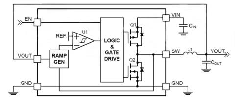
In order to keep the efficiency up in the 95 percent range for high-current applications, more complex circuit functionality with programmable switching frequency is required. Fairchild Semiconductor’s FAN2103 fully integrated synchronous buck regulator is intended for graphics card and set-top box applications. This device features a ‘power-good’ control signal; power down, over-voltage, under-voltage, and thermal protection; and an input under-voltage lockout control to avoid damage to the chip and the external components. All of these features come at some cost of pin count and external components, as is seen in Figure 4, which illustrates a typically application configuration.
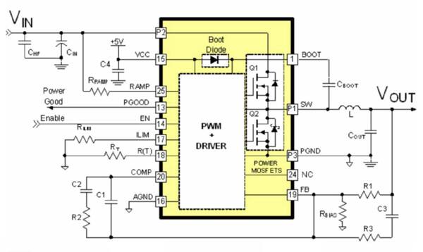
The large, 25-pin, molded leadless package (MLP) enables the FAN2103 to operate from -400C to +850C, though the device needs an external heatsink to operate at the upper end of the temperature range in extended operation. The device has a programmable output that supports standard ICs with known nominal voltages as well as custom chips that may have non-standard voltage requirements. These high-efficiency converters support input voltages upwards of 24 volts, so they can be directly run from wall transformer and line cord power supplies without additional power management.
DC-DC switching boost regulators
Boost regulators are primarily used to step up the output from a battery in the 3.3 to 5 volt range. Boost regulators use both external inductors and capacitors to dump charge and current into a capacitor to enable a higher output voltage. Figure 5 shows Fairchild Semiconductor’s FAN4860 synchronous boost regulator block diagram.
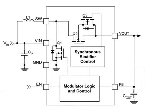
Like buck converters, boost converters have a thermal component that must be considered. The FAN4860 device has both voltage and thermal lockouts that force it to shut down when necessary. Since these regulators tend to be used in small-format devices, they are not generally used with heatsinks. As a result, the thermal stability of the capacitors and inductors must be in line with the system operating environment.
For short durations, loads designers may use a charge pump to create an increased voltage. Charge pump circuits are used for transient peak voltage and current applications. They make use of an external inductive or capacitive element as the charge storage device to hold the extra power while the new level is built up. This allows 3.3 or 5 volt systems to supply 12 volts, for example, for short durations. Unlike boost and buck regulators, which have a short start-up time, charge pumps have a per-use setup and discharge cycle. The quality of the power from the charge pumps is usually threshold based rather than regulated and deceases quickly with current drain.
Power considerations
However efficient they may be, PMICs dissipate power, which generates heat that must be conducted away from the device. To supplement the power management, PMICs use heatsinks, which increase the surface area in contact with the air flow of the system. The heat is spread out over multiple surfaces based on the shape of the heatsink and the shape of the component being cooled.
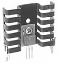
Heatsinks have to have a high degree of contact with the regulators to help channel the heat away. As a result, they must have strong mechanical connections. The majority are connected through heat-conductive adhesive or a bolt-on mechanical connection. For connection to the standard 3-terminal linear regulators in the TO-220 package, there are a number of fin shapes that connect via clip and/or bolt to the embedded power connection of the regulator. For example, heatsinks from Aavid Thermalloy (see Figure 6) are contoured to fit the TO-220 package and support both single- and dual-regulator configurations.
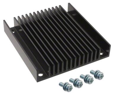
For switching regulators in SO and FlatPack packages, there are devices like CUI’s VHS-45 extruded heatsink. This device fits multiple FlatPack products and mounts to the PCB via four corner holes and bolts (see Figure 7). The heatsink is available in multiple sizes of fins based on the amount of heat to be dissipated and the amount of available air flow. The use of the heatsinks in fan-less mobile devices is limited, since they generally require a convective cooling airflow rather than a passive conductive flow.
Battery support
In addition to power regulation, mobile and portable systems need to have battery management. This function includes battery recharging as an integrated feature. Whether a system has a removable or a fixed battery, the need to perform in-operation charging is now a must. This task used to be quite a challenge to designers since the impact on state machine functionality was generally large. With the rise of embedded microcontrollers and microprocessors, the addition of battery charging circuitry is now straightforward. DigiKey has reference designs for the creation of battery fuel gauges which monitor both the power usage of a battery system and the recharging control.
Summary
As the portable device space adds new features, it also adds new power supply requirements and features. These power control devices utilize different techniques for regulation. The devices also feature a number of parameters besides voltage level, including the current output and thermal characteristics. These other parameters define the package size, heatsink, and duty cycle, which, in part, determine the industrial design of new mobile and consumer products.

免责声明:各个作者和/或论坛参与者在本网站发表的观点、看法和意见不代表 DigiKey 的观点、看法和意见,也不代表 DigiKey 官方政策。


