Microwatt ADCs Enable Energy-Harvesting Wireless Sensor Designs
投稿人:电子产品
2013-08-14
Wireless sensor systems powered by ambient energy harvesting depend on the use of the lowest power analog-to-digital converters (ADCs) available. For these systems, designers have typically had to contend with sacrificing measurement resolution to achieve low-power requirements. Now, however, engineers can find a range of low-power, high-precision ADCs from manufacturers including Analog Devices, Linear Technology, Renesas, and Texas Instruments, among others.
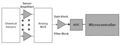
In multi- or single-channel energy-harvesting applications, engineers need to achieve required accuracy with limited power consumption in energy-constrained designs. As a result, low-power ADCs play a central role in the signal chain of a typical energy-harvesting wireless sensor design (Figure 1).

For sensor applications, delta-sigma (ΔΣ) ADCs offer distinct performance advantages including high resolution and high noise immunity. In addition, today's leading ΔΣ devices typically provide output that is fully settled after a single conversion. This zero-latency conversion capability contrasts with earlier generations of ΔΣ ADCs, which required designers to build in a waiting period for additional conversions before retrieving data when the analog inputs changed.
For low-power sensor applications in particular, however, input sampling currents can overwhelm high source impedances or low-power, low-bandwidth signal-conditioning circuits. More recent ΔΣ architectures address this problem through specialized methods. For example, Linear Technology uses a proprietary method to balance the input currents and thus simplify or even eliminate entirely the need for signal-conditioning circuits.
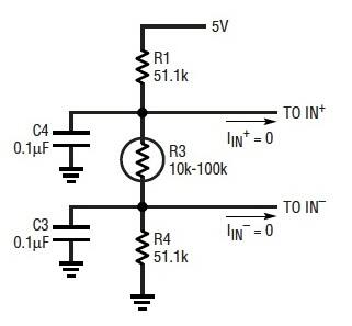
In a sensor application such as thermistor measurement, engineers can connect the ADC for direct measurement of thermistors up to 100 kΩ. Typically, the thermistor would be balanced to minimize input current (Figure 2). When resistors R1 and R4 are exactly equal, the input current is zero, reducing the chance of measurement errors. By eliminating the need for amplification, this approach is particularly well suited to low-power energy-harvesting applications.

At the heart of Linear Technology ADCs such as the LTC2484 and LTC2481, a proprietary sampling scheme automatically cancels differential input current, thus eliminating dynamic input current errors and on-chip buffering. As a result, engineers can design sensor systems able to deal with large external source impedances and directly digitize input signals across the full rail-to-rail input range while maintaining high accuracy.
The LTC2484 is a 24-bit ΔΣ ADC providing a four-wire interface comprising serial data output (SDO), serial clock (SCK), chip select (CS) and serial data input (SDI). The Linear LTC2481 provides similar functionality to the LTC2484, but with a 16-bit ΔΣ ADC and I²C digital interface.
Designed for ultra-low-power designs, both the LTC2484 and LTC2481 consume only 480 µW during full operation. Designers can achieve even lower power operation for low-frequency sampling applications by using single-conversion mode. As with other ADCs in this class, the LTC2484 and LTC2481 single-conversion mode causes the device to enter sleep state after the conversion is completed. While in this sleep state, power consumption for these devices drops significantly – by two orders of magnitude in the case of the LTC2484 and LTC2481.
For applications requiring more continuous conversion at low power, engineers can find a class of ADCs that consume less than 300 µW. For example, the Texas Instruments ADS1244 is a 24-bit ΔΣ ADC that consumes only 270 µW. As with other advanced ΔΣ ADCs, the ADS1244 can operate in single-conversion mode, operating in sleep mode with <1 μW power consumption between separate, zero-latency conversions. Engineers can set the ADS1244 to enter self-calibration mode immediately after waking from sleep mode – ensuring accuracy after relatively long periods of inactivity commonly encountered in energy-harvesting sensor applications.
The TI ADS1244 is designed to connect easily to MCUs such as the TI MSP430. The ADS1244 supports 2.5 to 5.25 V analog supplies and 1.8 to 3.6 V digital supplies. Nevertheless, engineers can configure the ADS1244 to operate with a single supply by connecting the AVDD and DVDD together for a 3 V supply – or use an external resistor to drop a 5 V supply down to a desired voltage level for DVDD.
Analog Devices offers a family of ultra-low-power ADCs including the AD7788/AD7789. Designed for low-frequency measurement applications, these devices typically use 65 µA (3 V supply) or 75 µA (5 V power supply). The AD7789 contains a 24-bit ADC with one unbuffered differential input, while the AD7788 is a 16-bit version of the AD7789.
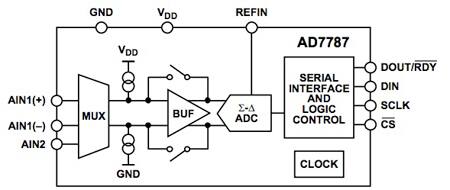
The Analog Devices AD7790 and AD7791 provide buffered versions of the AD7788 and AD7789, respectively. While unbuffered operation lowers the power consumption of the device, buffered mode allows engineers to place source impedances on the front end without contributing gain errors to the system. Analog Devices also offers the AD7787, a two-channel version of the AD7791 buffered 24-bit ADC (Figure 3).

In single-conversion mode, the AD7788/AD7789 (and AD7790/AD7791) switch to power-down mode between conversions. Power-down mode consumes 1 μA (max), allowing very low operation for low-frequency sampling requirements typically found in sensor measurement applications.
For applications that are not faced with high-resolution measurement requirements, engineers can also turn to MCUs that integrate relatively low-resolution ADCs. For example, 10-bit ADCs are integrated on-chip in MCUs such as the Texas Instruments MSP430F2132 or Renesas RL78 family, among others.
Designed to operate within a supply voltage range of 1.8 to 3.6 V, the TI MSP430F2132 features active-mode power consumption of 250 µA at 1 MHz (2.2 V supply), while consuming only 0.7 µA in standby mode and 0.1 µA in RAM-retention off mode.
The Renesas RL78 MCU family operates with supply voltages in the range 1.6 to 5.5 V, consuming 66 µA/MHz of current in normal run mode. The RL78 family includes devices with higher-resolution ADCs on chip, and all members offer a broad range of low-power modes. Among these available low-power modes the device can be programmed to allow the processor core to sleep while enabling operation of peripherals.
For example, engineers can program RL78 MCUs to perform ADC measurements that are triggered by the RTC timer without waking the CPU. While the CPU remains asleep, the device can compare the latest ADC results with preset upper and lower limits using a window comparator. If the ADC value falls outside the window, an alarm signal can wake the CPU to handle required processing tasks. This approach significantly cuts power requirements: While the device consumes 5 mA in run mode using the ADC, this snooze mode requires only 0.5 mA.
ADCs are essential to sensor designs, but in energy-harvesting applications, engineers need to balance power and performance capabilities to achieve the required measurement accuracy without overtaxing available power sources. Engineers can find a broad array of high-precision ADCs capable of operating below 500 µW or lower-precision ADCs integrated along with diverse peripherals in highly integrated MCUs. Using available ADCs and integrated MCUs, engineers can address a growing range of requirements for both measurement accuracy and low-power operation in energy-harvesting applications.
For more information on the products discussed in this article, use the links provided to access product pages on the DigiKey website.
免责声明:各个作者和/或论坛参与者在本网站发表的观点、看法和意见不代表 DigiKey 的观点、看法和意见,也不代表 DigiKey 官方政策。


 中国
中国