MCU-controlled Battery Management is Critical for Successful Internet of Things Implementations
投稿人:电子产品
2015-04-01
MCUs will be the main control element in most Internet of Things (IoT)-oriented designs and these MCUs will likely be battery powered. Power efficiency will be critical to achieving acceptable battery lifetime so the MCU will need to manage battery use with more precision than ever before. Many MCUs have special features that help manage battery power and using these features optimally may make the difference between winning or losing in the marketplace.
This article will quickly review some of the key features needed to implement efficient battery-based MCU design and will illustrate, using example devices, how these features improve efficiency and battery life. Software tools that help estimate battery lifetime will be used to show how to estimate lifetime prior to detailed design implementation. This helps dramatically with device selection and is a key technique for creating power-efficient designs.
Managing power domains
When thinking of battery-based MCU implementations we may initially have the assumption that there is a single MCU power domain, running off a battery and that our objective is to manage this power domain to create the most power-efficient MCU implementation possible. Soon we will discover that this assumption is usually false, however, and that even simple MCUs typically have multiple power domains on-chip. It turns out that having multiple power domains can be a big advantage when power efficiency is of primary importance to our design. Having multiple domains can allow us to more efficiently manage and control power to the portions of the MCU that are needed based on the functions we need to perform for our particular implementation. Let’s look at a specific MCU and see how multiple power domains can be advantageous to a typical battery-powered design.
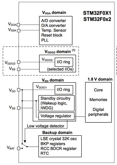
The STM32F0x1 MCU series (e.g., the STM32F051K8U6) is an entry-level device in the STM32 MCU family, and as such is a good example of a device that can be often used in battery-based applications. Figure 1 below shows the various power domains available for the STM32F0x1/x2 devices. The VDDA domain powers the analog-oriented blocks in the device and includes functions for the A/D converter, D/A converter, temperature sensor, reset generator, and the clock PLL. The VDDIO2 power domain is available on the STM32F04x/7x/9x devices and provides an independent I/O supply rail when different I/O standards need to be supported (this supply voltage can range from 1.65 to 3.6 V to cover a variety of I/O standards). The main VDD power domain provides power to the bulk of the device. This includes the I/O ring on the non-STM32F04x/7x/9x devices, the standby circuitry and wake-up logic that is usually always on and it also powers the 1.8 V digital core (processor, memory, and digital peripherals) via an on-chip voltage regulator.

Figure 1: STM32F0x1/x2 power sources showing battery backup domain. (Courtesy of STMicroelectronics)
The final power domain, sourced from the external VBAT pin, provides power to the backup domain. The backup functions include a low-energy 32 KHz crystal clock oscillator, the backup registers that retain their value even when power goes off to the rest of the device (handy for saving important data in between system resets and power fluctuations), and the real-time clock (RTC) block. A low-voltage detector can automatically switch to the VBAT input when the VDD signal is below a set threshold to simplify battery-backup implementation.
These separate power domains make it easy to control and manage the power delivered to the MCU depending on the operation required by the application. For example, if the device is waiting for the RTC to signal its time to begin an analog-to-digital, the majority of the device can be powered down with just the battery backup domain operating. The RTC timeout can switch an I/O signal to alert an external power-management device that can then turn on additional power domains. This can be a very power-efficient technique, but requires an external-power and battery-management device.
In some applications the STM32F0x1/x2 device will manage the battery and power to key blocks on its own by putting various sections of the device into low-power modes, managing clock frequencies and measuring voltage sources to detect when low-voltage levels may impact operations. In these applications multiple on-chip voltage domains and low-power operating modes are both key requirements. Let’s now look at low-power modes in more detail to see how they work with multiple on-chip power domains to further improve the power efficiency of battery-based implementations.
To assist engineers in design development STMicroelectronics provides a Product Training Module overview of its STM32F0 series.
Low-power MCU operating modes extend power efficiency
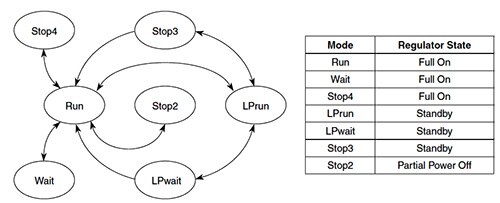
Just about every MCU now offers a variety of low-power operating modes that reduce operating power by restricting operating frequency and/or operability of key blocks. These modes have a variety of names, but their functionality is often very similar. The Freescale MCF51QE MCU series is a good example of the types of low-power operating modes you should look for when power efficiency is critical to your application. A state-transition diagram and a simple power-regulation table are shown in Figure 2 to illustrate how these modes can be used to improve power efficiency. The run mode does not restrict operations and the regulator operates in the full on-state. In the other modes various blocks operate using lower power by shutting down power to key elements or by reducing operating frequency. For example, in the Wait mode the CPU shuts down to conserve power but the peripherals operate at their full clock rate. This saves power when CPU operation is not needed, but timers or communications peripherals must continue to operate. Often these peripherals can just wake the CPU via an interrupt when the CPU is required. The ability to turn off the CPU saves a significant amount of operating power since the CPU, when operating, uses the majority of the MCUs power budget. A more detailed description of each low-power mode is provided in the section below.

Figure 2: Freescale MCF51QE128 low-power modes. (Courtesy of Freescale)
- Run mode — CPU clocks can be run at full speed and the internal supply is fully regulated.
- LPrun mode — CPU and peripheral clocks are restricted to 250 kHz CPU clock and 125 kHz bus-clock maximum and the internal supply is in soft regulation.
- Wait mode — CPU shuts down to conserve power; peripheral clocks are running and full regulation is maintained.
- LPwait mode — CPU shuts down to conserve power; peripheral clocks are running at reduced speed (125 kHz maximum) and the internal voltage regulator is running in loose-regulation mode.
- Stop modes — System (CPU and peripheral) clocks are stopped.
- Stop4 — All internal circuits are powered (full-regulation mode) and internal clock sources still at max frequency for fastest recovery.
- Stop3 — All internal circuits are loosely regulated and clocks sources are at minimal values (125 kHz maximum), providing a good compromise between power utilization and speed of recovery.
- Stop2 — Partial power-down of internal circuits; RAM content is retained. The lowest power mode for this device. A reset is required to return from Stop2 mode.
The run, wait, and stop modes are pervasive in modern MCUs and provide a basis for very-power-efficient designs. In particular, applications that only use the main CPU periodically – perhaps only to average a large number of sensor readings or to manage a received data buffer when the buffer is nearly full – can save dramatic amounts of power by turning off the CPU and letting intelligent peripherals handle as much of the algorithm as possible. The distinction between wait and stop is typically reflected in the response time since it usually takes much longer to power up a block from a low-power state (that reduces the static current in a typical stop mode) than to remove a clock gating signal to a block (that reduces only the dynamic current in a typical wait mode).
The LPrun and LPwait modes available in the MCF51QE128 provide another technique to reduce power consumption by running the CPU and/or the peripherals at much lower frequencies than normal. This is useful when operations are not easily implemented periodically and must be run continuously, but need not run at high speed. For example, a communications packet might be received at high speed in the normal run mode, but the LPrun could be used to process the data. This is particularly useful if processing time is data dependent and cannot be easily managed via a periodic timer interrupt. Once the data is processed, the LPwait state can be entered to wait until the next data packet needs to be received.
Using the various power domains and low-power modes in combination allows a wide variety of efficient implementations. Finding the optimal combination of various clock frequencies, low-power modes and state transitions can be a daunting exercise and usually needs to be done prior to detailed implementation or you may find you cannot meet your operating requirements using an already selected device and impacting project schedules significantly. Ideally you would want to be able to model the various operating power levels and estimate the battery lifetime for your target application. Luckily (or maybe because they understand this difficulty) MCU manufacturers have created some estimation tools we can use to solve this conundrum.
Software tools help estimate power requirements and battery lifetime
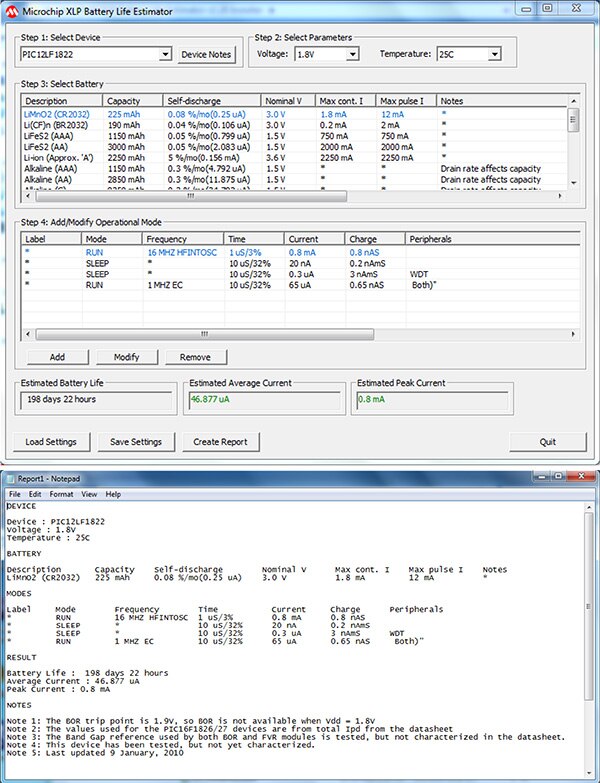
One of the easier to use tools is the Microchip XLP Battery Life Estimator (BLE)1. This free, downloadable tool works with any XLP MCU to estimate power consumption over the entire application. It can also be used to get detailed estimates for the power dissipation for key routines within your XLP MCU design. Figure 3 below shows the graphic user interface (GUI) for the BLE. You simply select your device, your voltage, and temperature and then your target battery (Steps 1 through 3 in the GUI). You can then specify the key operations in your application, defining the frequency of operation, the mode the function uses, the time the function is active and the various blocks (like ADC, UART, Timer, etc.) active during the function. (In the example below there is a function in the Run mode at 16 MHz, two sleep-mode functions and a run-mode function at 1 MHz) The software automatically determines the current used in each function and then reports the estimated battery life for the design. In the example, the battery life is estimated at just under 200 days. A complete text file report can be generated to save the program settings and results. An example is shown at the bottom of Figure 3.

Figure 3: Microchip XLP battery-life-estimator program – GUI and report. (Courtesy of Microchip)
Using a battery-life-estimator program makes it easy to identify the key routines and where your application uses the most power. This allows you to tune the design while trying different devices to find just the right implementation. Doing this prior to detailed coding and board design can save you from wasting significant effort exploring options that will not deliver the power efficiency you need for a successful design.
Once you have confidence in your selection you can then take the next step of using an evaluation kit, like the Microchip PIC24F Eval Kit. Typically these kits include a wealth of example code, reference designs, and extensive documentation to make it easy to code your key routines and measure the actual power levels you will get in a full implementation.
New low-power technologies for efficient battery-based implementations
MCU manufacturers are also pushing the technology envelope to continually create new low-power capabilities from the ground up. Texas Instruments has created a family of low-power-oriented MCUs using a new nonvolatile-memory Ferroelectric RAM, or FRAM, which combines the speed, flexibility, and endurance of SRAM with the stability and reliability of flash, all at lower total-power consumption. FRAM memory features ultra-low-power and fast (125 ns per word) writes. FRAM can be used as program, data, or storage to simplify application development. The ultra-low-power and non-volatility of FRAM makes it an excellent choice for battery-based MCU applications that require significant storage access and computation capabilities like data aggregation and sensor pre-processing.
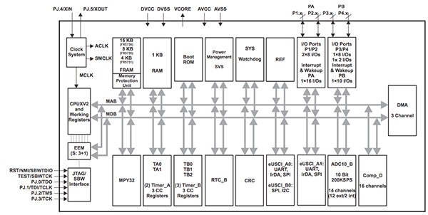
The MSP430FR MCU family also features key low-power modes, intelligent peripherals, and advanced processing capabilities. The block diagram in Figure 4 shows all the key MCU functions available in the MSP430FR5731/5/9 devices. Also check out the TI Product Training Modules that cover the features of the TI MSP430FR MCU Family and shows how the FRAM technology provides significant low-power advantages for a variety of applications.

Figure 4: Texas Instruments MSP430FR5731/5/9 block diagram. (Courtesy of Texas Instruments)
Conclusion
Many IoT applications will use battery-based MCU implementations and power efficiency will be critical for successful products. Selecting the right MCU for your implementation is easier when you use a power-estimation tool to select the right device for your target application.
For more information about the parts discussed in this article, use the links provided to access product pages on the DigiKey website.
References
免责声明:各个作者和/或论坛参与者在本网站发表的观点、看法和意见不代表 DigiKey 的观点、看法和意见,也不代表 DigiKey 官方政策。


 中国
中国