High Power Factor LED Replacement for T8 Fluorescent Tubes
投稿人:Convergence Promotions LLC
2011-05-27
LEDs are increasingly replacing incandescents in luminaires, but they have a great future replacing fluorescents, too.
This article describes the principles and design equations required for the design of a high brightness LED lamp using the AL9910 high-voltage LED controller. The equations are then used to demonstrate the design of a universal, offline, high power factor (PF), 13 W LED lamp suitable for use as a replacement for a T8 fluorescent tube. A complete design, including the electrical diagram, component list, and performance measurements are provided.
The AL9910 high power factor buck LED driver
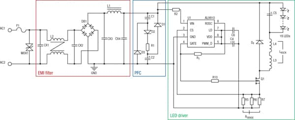
Figure 1 shows the electrical diagram of an offline 13 W LED driver.
On the input side, CX1, CX2, CX3, CX4, L1, and L2 provide sufficient filtering for both differential mode and common mode EMI noise generated by the switching converter circuit.
The rectified AC line voltage from the bridge rectifier DB1 is then fed into a passive power factor correction or valley-fill circuit, which consists of three diodes and two capacitors. D1, D2, D3, C1, and C2 improve the input line current distortion in order to achieve a PF greater than 0.9 for the AC line input.
The constant current regulator section consists of a buck converter driven by the AL9910. Normally, the buck regulator is used in fixed frequency mode, but its duty cycle limitation of 50 percent is not practical for offline lamps. This problem can be overcome by changing the control method to a fixed off-time operation.
The design of the internal oscillator in the AL9910 allows the IC to be configured for either fixed frequency or fixed off-time based on how the resistor RT is connected. For fixed off-time operation, the resistor RT is connected between the Gate and ROSC pins, as shown in Figure 1. This converter now has a constant off-time when the power MOSFET is turned off. The on-time is based on the current sense signal, and the switching adjusts to be the sum of the on- and off-time. This change allows the converter to work with duty cycles greater than 50 percent.
Design guide — high power factor offline LED driver
In this section the design procedure is outlined according to the schematic shown in Figure 1. First, guidelines for selecting the components for the valley-fill power factor correction stage and the fixed off-time buck converter are shown. The power inductor calculation is then demonstrated and finally, the power losses within the MOSFET and the free-wheel diode are assessed.
The specifications for the system are:
| VAC | = 230 Vac |
| VAC(min) | = 85 Vac |
| VAC(max) | = 264 Vac |
| ILED(nom) | = 240 mA |
| VLED(nom) | = 54 V |
| VLED(min) | = 42 V |
| VLED(max) | = 59 V |
| POUT | = 12.96 W |
| fswi(nom) | = 55 kHz |
Passive power factor correction stage design
The purpose of the valley-fill circuit (see Figure 2) is to allow the buck converter to pull power directly off the AC line when the line voltage is greater than 50 percent of its peak voltage.
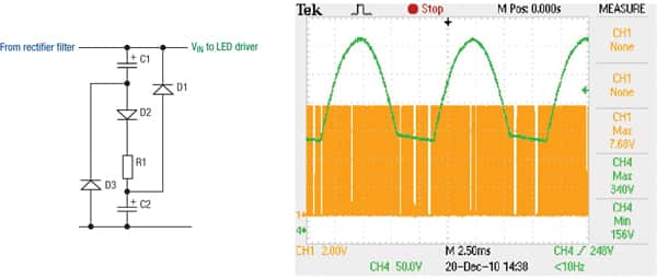
The following equation shows the maximum bus voltage at the input of the buck converter:

During this time, capacitors within the valley-fill circuit (C1 and C2) are in series and charged via D2 and R1. If the capacitors have identical capacitance value, the peak voltage across C1 and C2 is VIN(max) /2 = 186 V. Often, a 20 percent difference in capacitance can be observed between like capacitors. Therefore, a voltage rating margin of 25 percent should be considered.
Once the line drops below 50 percent of its peak voltage, the two capacitors are essentially placed in parallel. The bus voltage VIN(min) is the lowest voltage value at the input of the buck converter. VIN(min) at the minimum AC line voltage Vac(min) is as follows:

At 60 Hz, the total time of a half AC line cycle is 8.33 ms. The power to the buck converter is derived from the valley-fill capacitors when the AC line voltage is equal to or less than 50 percent of its peak voltage. The holdup time for the capacitors equates to tHOLD = 1/3 x 8.33 ms = 2.77 ms. The valley-fill capacitor value can then be calculated with the following equation:

Therefore, C1 = C2 = 15 μF. VDROOP is the voltage droop on the capacitors when they are delivering full power to the buck converter. Ideally VDROOP should be set to less than VDROOP = VIN(min) — VLED(max) in order to ensure continuous LED conduction at low line voltage. Nevertheless, VDROOP is set to be 20 V in the design example to avoid the need for a very large valley-fill electrolytic capacitor.
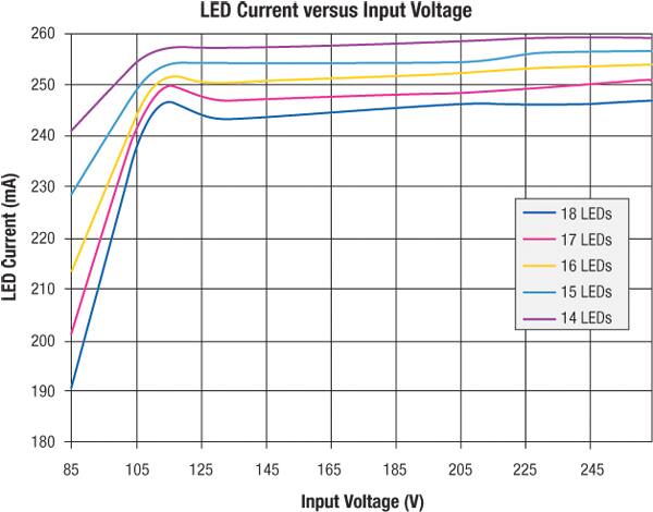
A VDROOP of 20 V implies that the bus voltage VIN at the input of the buck converter will drop to 40 V during part of the AC line cycle. As the buck regulator requires VIN to be greater than the LED stack voltage (VLED(max) = 59 V) for regulation, the LED will be off during part of the AC line cycle. This has the effect of reducing the actual output LED current at a low AC input voltage. In the design example, the LED current drops by approximately 20 percent from its nominal value at 85 Vac (see Figure 3).
Setting the fixed off-time and switching frequency range
For fixed off-time operation, the switching frequency will vary subject to the actual input voltage and output LED conditions.
A nominal switching frequency fswi(nom) should be chosen. A high nominal switching frequency will result in a smaller inductor size, but could lead to increased switching losses in the circuit. A good design practice is to choose a nominal switching frequency, knowing that the switching frequency will decrease as the line voltage drops and increase as the line voltage increases.
The fixed off-time tOFF can be computed thusly:

The off-time is programmed by timing resistor RT as shown in Figure 1. The value of RT is given by:

330 kω is selected for RT. Next, the two extremes of the variable switching frequency can be approximated as follows:


It is advisable to keep the maximum switching frequency fswi(max) below 150 kHz to avoid excessive switching loss.
Inductor selection and setting the LED current
The fixed off-time architecture of the AL9910 regulates the average current through the inductor LBUCK. The value of LBUCK depends on the desirable peak-to-peak ripple δIL in the output LED current. LBUCK can be set with the following equation:

Due to diameter limitation of the T8 tube, LBUCK is made up of L3 and L4 as shown in Figure 1.
The AL9910 constant off-time control loop regulates the peak inductor current Ipk. As the average inductor current equals the average LED current, the average LED current can be regulated by controlling Ipk.
Given a fixed inductor value, the change in the inductor current over time is proportional to the voltage applied across the inductor. During the off-time, the voltage seen by the inductor is the LED stack voltage. So, the peak inductor current should be regulated thusly:

The peak current is constant and set by the sense resistor RSENSE. If the LD pin is tied to the VDD pin, the value of RSENSE can be easily calculated because the voltage threshold on the CS pin is 0.25 V.

In the circuit shown in Figure 1, RSENSE consists of R5, R6, and R7.
The peak current rating of the LBUCK should be greater than Ipk and the RMS current rating of the inductor should be at least 110 percent of ILED(nom).
Although the described solution, working in fixed off-time and Continuous Conduction Mode (CCM), works as a constant current source, a limitation to the output LED current accuracy is its dependence on the number of LEDs and the overall LED chain voltage. The best result can be achieved using a fixed number of LEDs. A variable number of LEDs results in reduced current precision.
The two extremes of the output LED current can be approximated as follows:


The above equation shows that the precision of the LED current also depends on the tolerance of the practical inductor LBUCK. An inductor with a tolerance rating less than or equal to 10 percent should be chosen to ensure good LED current precision in mass production.
Power MOSFET calculation
The power MOSFET is chosen based on maximum voltage stress, peak MOSFET current, total power losses, maximum allowable working temperature, and the gate driver capability of the AL9910.
Maximum drain-source voltage stress on the power MOSFET for this converter is equal to the input voltage. However, a typical voltage safety margin for the MOSFET defines the maximum reverse voltage as follows:

This implies that a common 500 V MOSFET is suitable.
The power MOSFET losses will be dominated by switching loss. The switching loss depends on the switching time, frequency, MOSFET drain current, and drain-source voltage. The switching rise time tRISE and fall time tFALL are functions of the MOSFET’s gate capacitance, the gate driver capability of the AL9910, and layout design. The worst case switching power losses occur at VLED(min) and VIN(max). The switching loss is approximately:

The switching time tRISE and tFALL are measured to be 65 ns with the 600 V MOSFET SPB03N60S5 as the power MOSFET. As shown in Figure 1, R10 is a series gate resistor that slows down the MOSFET switching and reduces EMI emission.
The RMS current through the MOSFET at VLED(min) and VIN(max) is given:
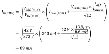
The power MOSFET conduction loss depends on its static drainsource resistance RDS(ON) at the MOSFET working temperature. It is possible to calculate the continuous conduction loss as:

The total power MOSFET loss is:

Total MOSFET power loss is dissipated from the SMD package into the PC board. So, it is possible to calculate the MOSFET working junction temperature if the package junction-to-ambient thermal resistance RthJA is known. The calculated MOSFET junction temperature, TJ, must be lower than the maximum allowable junction temperature TJ(MAX).

The internal ambient temperature within the LED converter, TAMB, is assumed to be 80°C. θthJA = 62°C/W is the thermal resistance for TO-263 with minimum copper area. For practical design, it is recommended to keep the junction temperature below 110°C to avoid temperature stress on the device.
Free-wheel diode calculation
The free-wheel diode DF, shown in Figure 1, is chosen based on its maximum stress voltage and total power loss. The maximum stress voltage rating of the free-wheel diode is the same as that of the MOSFET. It is advisable to use an ultra-low reverse recovery time TRR (<35 ns) diode as DF to reduce the MOSFET’s switching ON loss. In the design example, a 1 A 600 V rectifier, the MUR160, is selected.
The worst case average current through the diode occurs at VLED(max) and VIN(min).

Assuming a constant forward voltage drop VF across the diode, the conduction power loss can be calculated thusly:

Finally, the diode junction temperature without using the heat sink can be calculated:

The internal ambient temperature within the LED converter, TAMB, is assumed to be 80°C. θthJA = 32°C/W is the thermal resistance for the DO-201 package. For practical design, it is recommended to keep the junction temperature below 110°C to avoid temperature stress on the device.
The BOM shown in Table 1 lists the components needed to design a high power factor LED driver using the AL9910. The completed LED driver will fit inside a T8 LED fluorescent replacement lamp tube.
Results
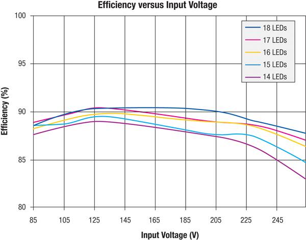
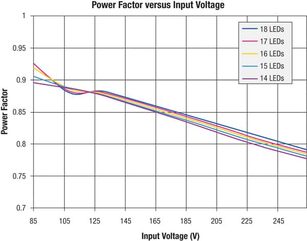
The performance of the system is outlined in Figures 3 and 4.
They display a level of system efficiency higher than 87 percent when driving 18 LEDs. The system efficiency is reduced with a decreasing number of LEDs, but an efficiency of 83 percent can still be achieved when driving 14 LEDs at 264 Vac input.
When driving 18 LEDs, a current regulation of around three percent is achieved between the input voltages of 110 Vac and 264 Vac. The LED current drops to 190 mA at 85 Vac as the minimum bus voltage VIN(min) falls below the LED stack voltage (VLED(max)) during part of the AC line cycle, driving the LED off.
Figure 5 shows the power factor across the line voltage range. A power factor greater than 0.9 can be achieved at 85 Vac.
| Ref. | Descriptions | Part Number | Package | Mfr. |
| U1 | Universal high brightness LED driver | AL9910 | S08 | Diodes Inc. |
| D1, D2, D3 | 1 A, 1 kV diode tRR=1.8s | S1M-13-F | SMA | Diodes Inc. |
| D4 | Ultra-fast-recovery diode 1 A, 600 V, tRR=35 ns | MUR 160 | DO201AD | Diodes Inc. |
| DB1 | 1 A, 600 V bridge rectifier | DF06S | DF-S | Diodes Inc. |
| C1,C2 | 15 µF, 450 V electrolytic capacitor +/-20% 1000 hrs @ 105°C | EEUED2W150 400KXW27M19X30 UCY2G150MPD |
5 mm pitch | Panasonic Rubicon Nichicon |
| C4 | 4.7 µF, 50 V electrolytic capacitor +/- 20% 1000 hrs @ 105°C, 10 mm diameter | ECE-A1HKG4R7 | 1.5 mm pitch | Panasonic |
| C5 | 10 µF 450 V electrolytic capacitor +/-20% 1000 hrs @ 105°C, 10 mm diameter | EEUEE2W100U | 5 mm pitch | Panasonic |
| CX1, CX2, CX3, CX4 | 100 nF, 275 VAC, Film, X2 | ECQU2A104ML | 17.5 mm pitch | Panasonic |
| F1 | 10 Ohm 1 W fusible resistor +/-200 ppm | NFR0100001009JR500 | Through-hole axial | Vishay |
| L1 | 6.8 mH inductor +/-10% 290 mA radial | 19R685C | 5 mm pitch | Murata |
| L2 | 30 mH common-mode inductor, 8 mm height | B82791G2301N001 | 10 mm pitch | EPCOS |
| L3, L4 | 3.3 mH inductor +/-10 percent 420 mA radial | 19R335C | 6 mm pitch | Murata |
| MOV1 | 275 V, 21 J, 9 mm, Radial | B72207S0271k101 | 5 mm pitch | EPCOS |
| Q1 | N-ch MOSFET 600 V, 3.2 A, Qg(max)=16 nC | SPB03N60S5 | TO263 | Infineon |
| R1 | 10 R 3 W wire wound resistor, 50 ppm/°C, +/-1% | UB3C-10RF1 | Through-hole axial | Riedon |
| R2 | 3 k 0.25 W resistor +/-5% | Any | 1206 | Any |
| R5 | 1R2 0.25 W +/-1% | Any | 1206 | Any |
| R6 | 2R7 0.25 W +/-1% | Any | 1206 | Any |
| R7 | 100 R 0.25 W +/-1% | Any | 1206 | Any |
| RT | 330 k 0.125 W resistor +/-1% | Any | 1206 | Any |
| R10 | 10 R 0.25 W +/-5% | Any | 1206 | Any |
Conclusion
This article provides a simple tool for designing an offline LED driver using the AL9910 high voltage LED controller. It provides a high level of efficiency as well as LED current control over a wide range of input voltages. Moreover, the article explains how to design a system with passive power factor correction to achieve a PF greater than 0.7, allowing compliance with emerging international solid state lighting standards.

免责声明:各个作者和/或论坛参与者在本网站发表的观点、看法和意见不代表 DigiKey 的观点、看法和意见,也不代表 DigiKey 官方政策。





 中国
中国