Clock and Data Recovery: PLLs Clean, Re-clock Timing Signals in Wireless Links
投稿人:电子产品
2016-01-26
Phase-lock loops are among the most versatile of circuit functions. They are used for clocking processors (a fairly benign situation), as well as for establishing tuning in fixed- and tuned-frequency transmitters and receivers.
However, among their most difficult challenges is recovering, cleaning, and re-clocking timing signals in wireless links. Unlike a processor clock, here the channel’s clock signal is not an explicit or separate signal, but is embedded within the modulated data stream. Even if both transmit and receive clocks are individually perfect and also perfectly synchronized (which is never the case), the channel will have noise, attenuation, varying SNR, distortion, and many other corrupting factors.
Besides their use in wireless channels, PLLs play a similar role for wired and optical-fiber links. In the two latter cases, the received signal is usually less corrupted and more stable compared to wireless, thus easing the task somewhat, but the data rate is often much higher (tens of Gbps for some optical links) which aggravates the challenge. Thus, the PLL must overcome different difficulties depending on the channel medium.
The complexities of the clock-recovery challenge are shown clearly in the most useful diagram associated with a communications channel, the eye diagram (Figure 1)1. This diagram overlays all the received bits of the data stream in real time, thus building up a composite which shows the degree of timing jitter, distortion, and attenuation at the receiver.
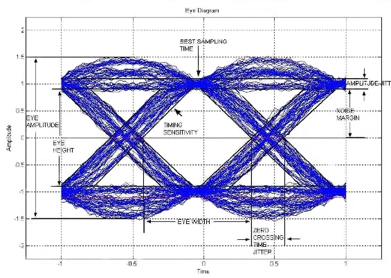
Figure 1: The eye diagram, an overlay of all the received data bits using the recovered system clock, reveals considerable information about jitter, attenuation, distortion, and many other characteristics of the received signal compared to the “ideal” digital signal it represents. (Courtesy of Yellow Fourier Technologies Private Ltd.)
While an ideal data bit looks like a square wave, any real bit has non-vertical slopes and rounding as its minimum imperfections; in addition, a real received signal will have all sorts of jitter, distortion, and attenuation. As the bits stretch out in time due to channel limitations, they overlap and the result is intersymbol interference (ISI) which makes it more difficult to achieve low bit-error rate (BER).
Therefore, the receiver must extract the timing of the data clock from the received modulated data stream despite many corrupting factors. Formally, this function is called “clock and data recovery” or “clock and data retiming” (CDR), but it is often described by the slang phrase “clock cleaning.” The receiver circuitry uses this recovered timing to determine the optimum instant to sample the data. The objective is to achieve the lower bit-error rate on the received bit values.
The PLL
The PLL uses a closed-loop negative-feedback topology to match the received signal’s embedded clock to a standard, locally generated clock (Figure 2). The principles and operation of PLLs has been covered extensively in technical articles, books, and websites, with explanations spanning mostly verbal, intuitive approaches all the way to those which provide intense mathematical analysis2,3 (the PLL is a good candidate for this level of investigation, as it can be accurately modeled). While PLLs were all-analog circuits for many years, they are now often implemented with digital circuitry (for example, the analog VCO is replaced by a numerically controlled oscillator); at higher frequencies, analog is still the only viable option.
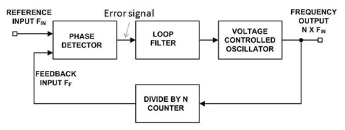
Figure 2: The basic PLL is a closed-loop, negative-feedback design which compares a locally generated phase/frequency with the received signal’s phase/frequency, and adjusts the VCO via a filtered error signal to track the input signal.
In all PLL applications, the specifics of the loop filter are critical to proving the overall performance needed. The primary filter parameter, of course, is bandwidth, followed by factors such as damping, roll-off steepness, passband ripple, and out-of-band attenuation.
A narrower bandwidth will result in less jitter on the recovered clock output, which is a good thing. However, this same narrow bandwidth means it will take the loop longer to initially acquire the received signal and lock it in when that signal undergoes shifts in frequency. In wireless links, these shifts often occur due to multipath, distortion, propagation delay issues, or even the Doppler Effect (which can be significant even at terrestrial speeds—think of radar speed guns).
Wireless links have further challenges, as well. For wired and optical links, the end points and the medium are usually fixed in place, so many of the corrupting influences are relatively static; for wireless links, one or both endpoints may be moving and the channel itself is changing, so the received signal undergoes many changes in real time. Therefore, the loop filter must be designed for a dynamic environment, beyond the standard issues such of noise and attenuation.
Obviously, the parameters of PLLs and their filters used for high-speed wireless links are initially set for the most likely channel conditions. Designs for very difficult situations sometimes do not use a single fixed filter, but instead use a more advanced one with time constants and other parameters that can be dynamically adjusted “on the fly” to match conditions.
CDR ICs matched to target applications
For many wireless applications – especially mass-market consumer ones such as Wi-Fi nodes – the CDR PLL is embedded in a larger IC which provides nearly the entire front-end functionality (although the receive-channel LNA [low-noise amplifier] and transmit-channel power amplifier [PA] are usually separate, discrete devices). However, CDR PLLs for higher-speed links are often standalone, limited-functionality devices to meet their performance requirements
The Exar XRT91L33 is one such example (Figure 3). This IC is designed for SONET/SDH 622.08 Mbps STS-12/STM-4 or 155.52 Mbps STS-3/STM-1 applications and implements the CDR function by synchronizing its on-chip voltage-controlled oscillator to the incoming serial non-return to zero (NRZ) data stream. The PLL locks to the local reference clock on startup. Once it achieves lock, it then attempts to lock onto the incoming data stream.
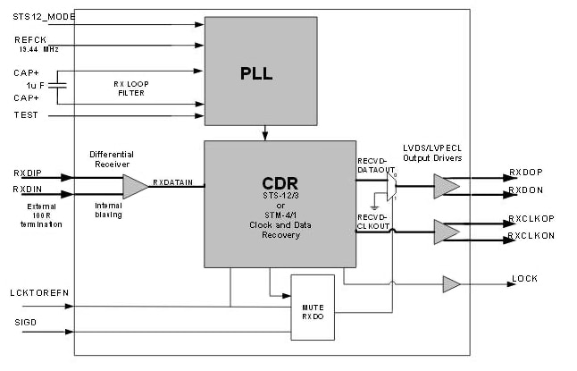
Figure 3: Exar’s XRT91L33 for SONET/SDH 622.08 Mbps STS-12/STM-4 or 155.52 Mbps STS-3/STM-1 applications provides clock data and recovery and also has a “fall-back” position in case the signal is lost or lock cannot be achieved for any reason.
Recognizing that there may be periods of lost signal, whenever the recovered clock frequency deviates from the local-reference clock frequency by more than approximately ±500 ppm, the clock-recovery function switches to the local-reference clock, concludes there is a loss of lock, and pulls the LOCK output pin to a low state. The user supplies the external filter capacitor for this 3.3 V, 20-pin TSSOP device, to match the anticipated situation.
Another example is the ADN2855, a burst-mode clock and data-recovery IC from Analog Devices which can operate at 155.52 Mbps, 622.08 Mbps, 1244.16 Mbps, or 1250.00 Mbps data rates (selectable via the I2C interface). As shown in Figure 4, it is designed for GPON/BPON/GEPON optical-line terminal (OLT) receiver applications. The ADN2855 requires a reference clock that is locked to the incoming data frequency; in operation, the IC’s loop acquires frequency lock with respect to this reference clock, pulling the VCO towards 0-ppm frequency error. As with the Exar part, the loop-filter capacitor is user-supplied, with a nominal value of 0.47 μF.
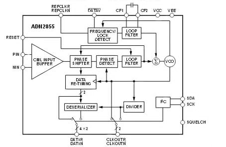
Figure 4: The ADN2855, a burst-mode clock and data-recovery IC from Analog Devices, operates up to 1250.00 Mbps data rates; the user-supplied filter capacitor has a nominal 0.47 μF value.
Targeting a different class of applications, the CDCM7005 from Texas Instruments is a radiation-tolerant (version CDCM7005-SP), low-phase-noise and low-skew clock synchronizer and jitter cleaner that synchronizes a voltage-controlled crystal oscillator (VCXO) frequency to one of the two reference clocks; the VCXO clock operates up to 2 GHz. The ruggedized IC is certified to 50 kRad (Si) TID, and QML-V Qualified per SMD 5962-07230, and can operate over the full military temperature range (–55°C to 125°C Tcase).
The PLL loop bandwidth and damping factor can be adjusted to meet different system requirements through the selection of external VC(X)O and loop-filter components. Phase noise is below 140 dB at frequencies between 10 kHz and 10 MHz (Figure 5). There are two PLL lock indications: a digital-lock signal or the analog one. Both signals indicate if the PLL achieves or loses lock according the user-selected lock condition. Like the Analog Devices PLL, many operating parameters are user-set via serial bus; here, the SPI bus.
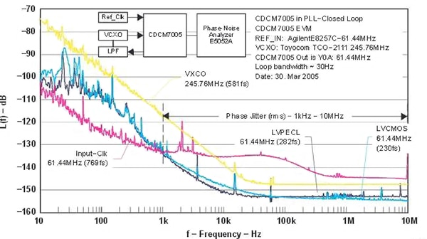
Figure 5: The CDCM7005-SP from Texas Instruments is a radiation-tolerant PLL which synchronizes a voltage-controlled crystal oscillator (VCXO) frequency to one of the two reference clocks, and operates up to 2 GHz.
Summary
The phase-lock loop has repeatedly proven to be one of the most useful and versatile topologies serving many aspects of electronic systems. Among these are frequency synthesis, tuning and channel setting, processor clocking, and received signal clock and data recovery. In this last area, it must extend its role from taking and transforming a known signal in a well-defined situation, to trying to extract a key timing component from a received signal which is somewhat known but has many unknowable distortions, drifts, and imperfections. Regardless of link medium, the PLL must re-establish some order from the received chaos. A properly designed PLL can do this and PLLs have a proven track record in the CDR applications, enabling data recovery with low BER despite severe signal challenges.
For more information about the parts discussed in this article, use the links provided to access product pages on the DigiKey website.
References
- R.W. Lucky, J Salz, and E.J. Weldon, Jr., Principles of Data Communications, McGraw-Hill
- Gardner, Floyd M. (2005), Phaselock Techniques (3rd ed.), Wiley-Interscience, ISBN 978-0-471-43063-6
- Viterbi, Andrew J., Principles of Coherent Communications, McGraw-Hill.
Further Reading
- Texas Instruments, AN-46 The Phase Locked Loop IC as a Communication System Building Block
免责声明:各个作者和/或论坛参与者在本网站发表的观点、看法和意见不代表 DigiKey 的观点、看法和意见,也不代表 DigiKey 官方政策。




 中国
中国