Actively Seeking a Better ORing Solution
投稿人:DigiKey 欧洲编辑
2012-03-13
Active ORing offers significant benefits using MOSFETs over Schottky diodes, but it does impose some design parameters that engineers need to appreciate in order to develop the most appropriate solution.
The use of diodes to actively combine multiple or redundant power sources is a technique that spans the history of the semiconductor industry, as the diode is one of the simplest and most useful semiconductors in use today. Its simplicity, however, is also its downfall in this class of application, thanks to the 'crowbar' effect of a forward-biased PN junction. While there is now a range of diodes with different switching characteristics from which to choose, such as power Schottky diodes, the basic functionality remains ‘on’ or ‘off’, belying the main benefit of a semiconductor junction: control. Due to the fundamental physics of a diode’s PN junction, the more current they pass the more power they dissipate.
Replacing the humble diode with the more sophisticated field-effect transistor lowers the power dissipation and introduces a level of control not possible with the diode, but it too has its consequences. Understanding those consequences has enabled the semiconductor industry to develop a range of control solutions for using MOSFETs in active ORing topologies.
Active ORing is now commonplace in power supply design, but is most relevant in applications that must match the needs of delivering significant levels of power with a high degree of ruggedness and reliability. Today, that typically points towards telecommunications, but it is equally valid in other applications where load sharing/balancing between power supplies is implemented, or where so-called 'N+1' redundancy is required.
Conceptually, replacing diodes with MOSFETs is relatively straightforward and brings instant benefits in terms of reliability. The power dissipated by a diode when it is conducting is significant and proportional to the current passing through it, so in high power applications, the diodes tend to dissipate higher power. In turn, this demands the use of larger diodes and heat sinks, or other cooling solutions such as forced air or convection. Wherever cooling becomes necessary, it represents a potential point of failure. So, as the heat dissipated by diodes increases, so too does the risk of failure. It is widely accepted that despite the efforts to lower the active power consumption of integrated devices, the power demand trend of today's applications is only increasing, thereby demanding ever more powerful power supplies and, in turn, larger diodes with their associated heat dissipation issues.
To overcome this problem, the industry has moved over to using MOSFETs as they dissipate significantly less power than their diode counterparts - in many cases as much as ten times less. The benefits are clear – less power dissipated means lower cost solutions, as well as higher reliability. However, while the total cost of ownership may be lower, the BOM costs are potentially higher, as not only is a MOSFET needed for every diode replaced, but each MOSFET potentially needs its own control IC to monitor and regulate their operation. While the cost and selection of MOSFETs is vast, the same is not necessarily true for the control circuits. As a result, engineers must now turn towards their careful evaluation and selection.
Basic ORing solutions
The concept of active ORing is flexible: the MOSFETs may be positioned on the power rail (high-side) or in the return path (low-side), and within either the power supply or the application. The topology chosen will influence the choice of controller, but high-side approaches are predominantly favored. Attention must now turn towards functionality. Simpler controllers provide a basic level of control, essentially mimicking the forward-bias effect of a potential difference across a PN junction. Obviously a MOSFET's channel does not start conducting simply due to the presence of a potential difference between its source and drain terminals; it needs a gate bias in order to start conducting. This is crucial to the operation of active ORing, but it also imposes the need to detect and respond to operational and fault conditions. Using a traditional diode approach, the power supply is protected by a fault condition due to the polarity reversal across the PN junction. The time taken for the diode to stop conducting is probably the most crucial parameter to consider when selecting a diode. For a MOSFET, that response must be applied by the controller so it is necessary for it to sense the forward voltage drop developed across the channel (VSD). In order to do this, the controller will typically feature a sense input that is fed via a sense resistor - normally this is implemented using a comparator integrated alongside the logic and drive circuitry within the controller.
The comparator's performance will depend almost entirely on the excursion of VSD; the smaller the forward voltage drop, the more difficult it will be for the controller to reliably measure. The consequence of this is that under a fault condition, the controller's response time to a change in VSD will directly impact the speed with which it can turn off the MOSFET under that fault condition. This leads to perhaps the most significant trade-off an engineer will face when selecting the right MOSFET for a given application. It is tempting to opt for the lowest possible RDS(ON) because the lower the RDS(ON) of the MOSFET, the lower the power dissipation under full load. Typically, N-Channel MOSFETs are not just a lower cost option over P-Channel, but they offer a lower RDS(ON) too.
However, a lower RDS(ON) also dictates the VSD parameter and, in turn, the switch-off speed of the controller under fault. For this reason many manufacturers will feature the sense voltage as a key parameter in their datasheets. As an example, consider the IR5001S (Figure 1) from International Rectifier, a relatively basic controller targeting high side designs which offers a VSD of 50 to 100 mV. This allows for the selection of low-cost N-Channel MOSFETs, while offering an output delay time of typically 0.8 μS. This device is designed for use in parallel, requiring one controller for each MOSFET, and is suitable for both input- and output-ORing designs.
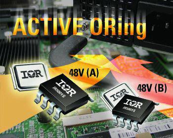
Figure 1: International Rectifier’s IR5001 controller.
Another feature of active ORing is the ability to detect and compensate for the load current, balancing it across multiple power sources. Linear Technologies’ LTC4357 not only offers a turn-off time of just 0.5 μS, but operates with a typical VSD of 25 mV. When configured in a load sharing configuration (Figure 2), the LTC4357 employs load sharing as a function of RDS(ON) as well as the impedance of the supplies and their initial output voltages.
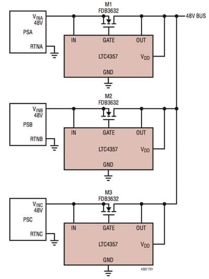
Figure 2: Typical load sharing configuration using the LTC4357 from Linear Technology. (Source: Linear Technology Datasheet)
Feature-rich ORing
For applications that demand greater control or a wider selection of features, there is a new generation of active ORing controllers that offer extended functionality. As well as the essential ORing features, some provide additional value-added options. For example, the MAX5963 from Maxim is a dual Hot-Swap and diode ORing controller with an operational range of between 7.5 V and 76 V. Its features allow it to target a specific range of applications including blade servers, base station line cards, network switches/routers, and FireWire ports/hubs. Specifically, it provides independent load current limiting for each channel, with load disconnect. This feature means it can also offer a user-controlled shutdown mode which limits its own power to just 10 μA. In operation, it can limit the output current. If the load current exceeds its set value, the output current is actively limited for a time period set using an internal 1/128 integrating timer, which is adjusted via an external resistor (Figure 3). Once the time limit is exceeded, the MAX5963 can be configured to either retry or latch the channel off. The device also provides fault status outputs; two high-voltage, open-drain outputs that pull low when either a current limit or circuit breaker fault is detected.
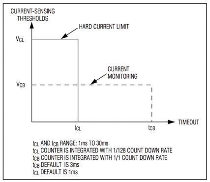
Figure 3: Functional block diagram of the MAX5963’s internal integrating timer. (Source: Maxim Datasheet)
Fault detection is also a feature of Intersil’s ISL6144. Figure 4 shows the block’s structure, which is capable of detecting five discrete fault conditions: ORingFET off due to dead short in the sourcing supply leading to VIN<VOUT; shorted terminals of the ORingFET; blown fuse in the power path of the sourcing supply; open Gate terminal; and an undervoltage. Unlike the MAX5963, the Fault pin is not latched, so it is only active-low while a fault exists. The ISL6144 is able to support this level of diagnostics thanks to the extended features it integrates, such as an undervoltage comparator, but it also features other functions not found on all controller ICs including a hysteretic regulating amplifier.
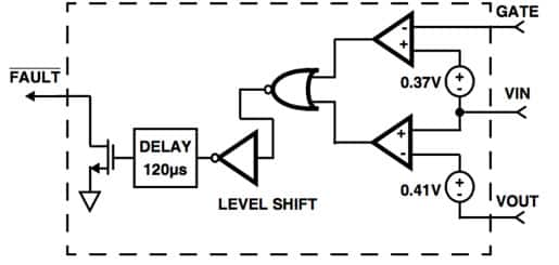
Figure 4: Fault detection block of the ISL6144 from International Rectifier. (Source: International Rectifier Datasheet)
Diode ORing is a well-established but fundamentally limited technique, particularly in high voltage systems. The widespread adoption of active ORing using N-Channel MOSFETs is driving innovation, resulting in a more varied and optimized approach to the problem. Continued developments in this area are sure to help drive not only power efficiency in embedded design but improved overall reliability in end products.

免责声明:各个作者和/或论坛参与者在本网站发表的观点、看法和意见不代表 DigiKey 的观点、看法和意见,也不代表 DigiKey 官方政策。





 中国
中国