iCE40 FPGA Calculator (Beginner)
2023-12-15 | By Ethan Nichols
License: Attribution Switches
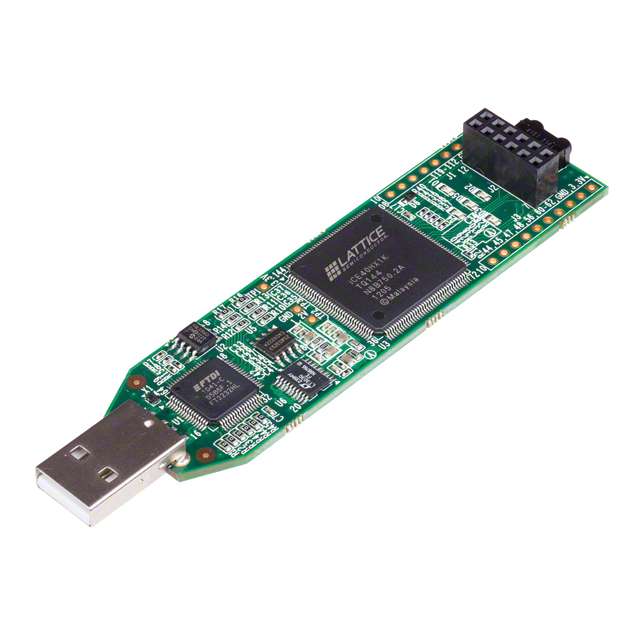
At $50, the iCE40 icestick FPGA development board sits at the top of my list of starter FPGAs. Shawn Hymel’s video series on DigiKey’s YouTube channel explains the board wonderfully, and I have three techniques to help you get started more easily. Although you don’t need to watch his first video on theory, I would recommend watching his second video before you read this article. This article also covers some more in-depth tools for digital logic design that will be much more helpful after Shawn Hymel’s video shows you the fundamentals.
Tips And Tricks for Getting Started
First, I made sure to download the latest versions of Python and Apio. Before the developers updated Apio, Shawn Hymel's video recommended using an older version to prevent bugs, but as of August 2023, the latest versions of Python and Apio work correctly together.
Second, instead of showing Lattice Cable for the icestick device on Zadig, my computer shows “Dual RS232-HS.” I fixed this issue by replacing Lattice Cable with the Dual HS name in a *.json file. In two minutes, you can easily fix this issue by viewing the GitHub Issues page below.
https://github.com/FPGAwars/apio/issues/305
Link to GitHub Issues page for this problem
Image of the Dual HS name where the Lattice Cable name used to be.
Third, you may get a strange error [shown below]. When this happens, re-downloading the driver for the icestick—just like Shawn Hymel shows in his second video—fixes the issue.
Choosing my project
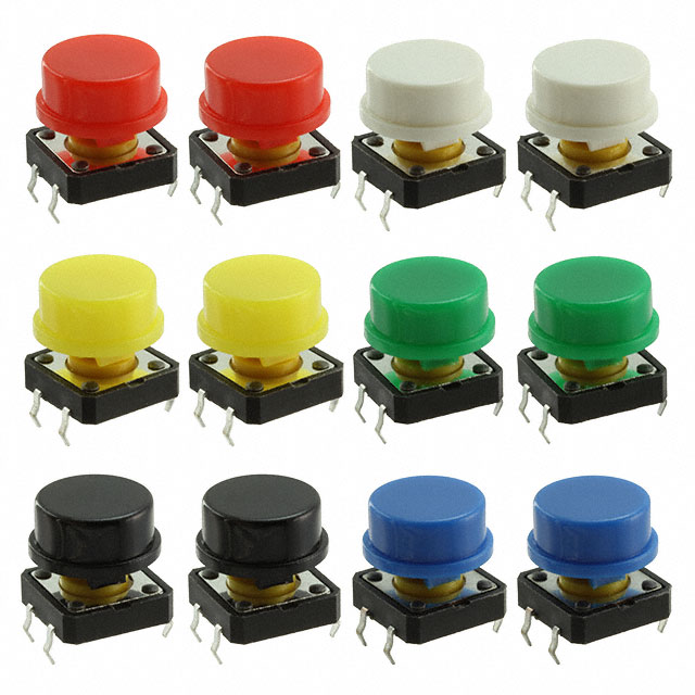
Once I had all the software installed, I chose a project. Since FPGAs have logic gates as their building blocks and I have an easy time visualizing calculators with logic gates, I settled on building a calculator to multiply two 2-bit numbers. I used four switches: two on the left for one number and two on the right for the second number. The LEDs on the icestick show the result.
Since I have taken two digital logic classes, I knew I had three special tools for the project: truth tables, Karnaugh maps, and logic gate schematics. Each tool I used in this process let me see a different perspective on this project's logic and helped me reduce the number of gates.
My teacher in college had good insight. More gates make your design more complicated and harder to debug. If you’re using FPGAs, you’re taking up more space on the chip, and if you’re using logic gate chips, each gate could cost you, for instance, $0.25. If your design were to be mass-produced, those $0.25 could cost the manufacturer thousands of dollars more. Whether or not we design for manufacturing, we can have fun challenging ourselves to see how efficient we can make the design!
Truth tables
First, I drew my truth table. This table looks overwhelming, but in the next step, we’ll break it down into four more manageable pieces. For now, I went through each combination of inputs and asked, “What result am I expecting?” For instance, if I press buttons A and C, the computer sees an input of "1010" and knows to multiply the first "10" by the second "10." In decimal numbers, the calculator will multiply 2 by 2. The LEDs then show the user the answer in binary, which is "0100."
Karnaugh maps
Second, I broke the truth table into four smaller Karnaugh maps (K-maps). These maps help us see the patterns in the digital logic.
From each K-map, we can find a Boolean expression.
X = ABCD
X_out is the easiest; since A, B, C, and D are all 1 when X is 1, we get the expression X = ABCD. This is an AND gate, and this expression tells us that if switches A, B, C, and D are all 1, then LED X will be 1.
Y = AB’C + ACD’
The 1 at the corner is “used" twice. The AB’C comes from the two bottom 1’s, and this term tells us that if A is on, B is off, and C is on, then LED Y will turn on. The ACD’ comes from the two 1’s on the right, and this term tells us that if A is on, C is on, and D is off, then LED Y will also turn on. The “+” is an OR gate, meaning that if either AB’C or ACD’ is true, then LED Y will turn on.
Z = ABC’D + ACD’ + A’BC + AB’C = (A ^ B)C + ABC’D + ACD’
As shown with the red circles grouping the 1’s, Z_out had more complexity. Each circle represents a different AND gate, and they’re all joined by an OR gate. You can overlap the circles; just keep in mind that the more circles you have, the more gates you use. Remember: fewer logic gates make the project cheaper to produce in the business world.
N = ABD + A’BC
N_out’s explanation shares similarities with Y_out’s explanation. Since the two bottom left 1’s are grouped together and the top right two 1’s are grouped together, there are two terms, joined by an OR gate. Pay careful attention to the AB and CD columns on the K-map, and the table will tell you
For more information about Karnaugh maps, All About Circuits has a fantastic article:
https://www.allaboutcircuits.com/textbook/digital/chpt-8/introduction-to-karnaugh-mapping/
Logic Gates
Third, I drew the logic gates. I included an image of the logic gates using OrCAD for you to read more easily, but I drew them on paper when I designed the project.
OrCAD's EVAL library used to draw the logic gates.
We can imagine each of these four inputs (A, B, C, and D) as switches already, and we can use this schematic to predict which LEDs (X, Y, Z, or N) should light up.
I noticed when I tried my first Verilog file that I needed a NOT gate on every input to get the results I expected. My best guesses: either the pull-down resistor inverts each input, or the icestick uses negative logic. Either way, the designer inverted the logic of the inputs.
Since I tried to synthesize the whole project at once instead of taking it in bite-size pieces, this project took me 16 hours over the course of four days and frustrated me. However, once I broke up this project into four pieces, I fixed it in one afternoon. Knowing the fundamentals and practicing them are two different things.
Using each of these three tools, we can test our circuit to see if it works!
Writing the Verilog
In every project that I use code, I start the project with a piece of code that I know works; I never start from scratch. By the end of the project, my code and the starting code were vastly different, but the starting code gave me a working framework to build on. For this calculator, I started with the LED *.pcf file from Lattice’s website and a Verilog file from my classmate, Andrew. Test benches are important, but this project does not use a test bench.
The approach Andrew and I take from our digital logic class differs from Shawn Hymel’s approach. Both methods declare our inputs, outputs, wires, and gates; but I use my college method since it’s more comfortable and clearer to me.
https://github.com/tempest1140/EthanN_MultiplicationCalculator
Final Verilog files
To clarify, you can plug this folder into your project path to run it; you don’t have to make any modifications.
Conclusion and Lessons Learned
After finishing this project, I learned three important lessons:
- Break the project into bite-size pieces
- Take breaks if you get stuck for longer than 20 minutes
- Check which buttons and LEDs you assigned to each port

Have questions or comments? Continue the conversation on TechForum, DigiKey's online community and technical resource.
Visit TechForum


 中国
中国