What Are PCBs and How Are They Made?
2024-05-29 | By Sarah Aman
Introduction:
Printed Circuit Boards, also known as PCBs, are the heart of any of the electronic devices that we use in our day-to-day lives. PCBs are in everything we use from our smartphones to our computers, and even some household appliances. In this article, we will examine what PCBs are, why they are important, and how they are manufactured.
What Are PCBs?
A Printed Circuit Board (PCB) is a flat board made from an insulating material of some kind. Usually, they are made from fiberglass, but other materials can be used as well. PCBs also have thin layers of conductive material etched into the surface. These conductive material layers are called 'traces' and are usually made from either copper or silver. These traces act as electrical pathways like a wire on a breadboard that connects various electronic components such as resistors, capacitors, integrated circuits, and transistors. This allows all the components to work together to form a circuit.
Why Are PCBs Important?
PCBs play an important role in the world of electronics for many reasons:
- PCBs facilitate the efficient and organized placement of electronic components. This eliminates the need for complex wiring and soldering.
- PCBs allow for components to be placed more tightly together to save space, which saves money and allows for complex devices like cell phones to fit in our pockets.
- PCBs provide a consistent and replicable design that ensures fewer errors and less time spent debugging. They also allow for better and faster mass production of electronic devices, which has brought us directly into the digital age.
- In the case of a malfunction, PCBs are easier to troubleshoot and repair than the normal tangled mess of wires many of us are used to.
How Are PCBs Made?
Creating a PCB is a multi-step process that combines technology, precision, and quality control. There are twelve key steps when it comes to manufacturing a PCB.
- Design and Layout: The PCB design is created using specialized software where the position of each component, the traces, and any additional features like drill holes are planned out. This design file serves as the blueprint for the entire manufacturing process.
- Substrate Material Selection: The choice of the substrate (base) material is very important. Most PCBs are made out of fiberglass-reinforced epoxy laminates, but other materials like ceramics or more flexible materials can be used based on the requirements of the device.
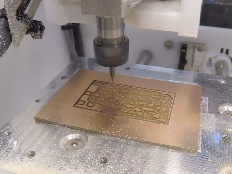
- Cutting and Shaping: The chosen substrate is cut into the desired size and shape. This forms the base of the PCB. This process can involve mechanical cutting or laser cutting for increased precision.
- Copper Cladding: One or both sides of the substrate are coated with a thin layer of copper which creates the conductive surface for the PCB. The copper is then cleaned, and a layer of protective film is applied to prevent oxidation.
- Photoengraving: A photosensitive material called the resist is applied to the copper layer. The PCB design is then printed onto a transparency, which is used to expose the resist to ultraviolet light. This process hardens the resist in the desired pattern.
- Etching: The unexposed resist is washed away leaving behind the copper traces defined by the PCB design. The PCB is then immersed in an etchant (a corrosive material that wears away layers of the material). Usually, a solution of ferric chloride is used. The etchant removes the exposed copper only leaving the desired copper traces.
- Drilling: Holes are drilled into the PCB to accommodate components and connectors. CNC machines are commonly used for high-precision drilling.
- Through-Hole Plating (Optional): For multilayer PCBs, a process called through-hole plating may be employed. It involves electroplating the holes with copper to create connections between the layers.
- Solder Mask Application: A solder mask is applied over the entire PCB, leaving only the copper pads exposed. The solder mask protects the copper and defines where solder can be applied during component assembly.
- Silkscreen Printing: Component labels, logos, and other identification markings are printed on the PCB's surface for reference by the user.
- Component Assembly: Electronic components are then soldered onto the PCB. This can be done manually or by using an automated assembly machine, depending on the complexity of the PCB and the production volume.
- Quality Control and Testing: Finally, each PCB undergoes rigorous quality control and testing to ensure it meets the required specifications and functions intended for it.
Conclusion:
PCBs enable the entirety of our world of electronics. They bring to life the complex devices that have become integral to all aspects of daily life. The manufacturing of PCBs is a meticulously orchestrated symphony of design, precision, and quality control. Understanding the intricacies of PCB production helps us to understand the remarkable technology that surrounds us.
Have questions or comments? Continue the conversation on TechForum, DigiKey's online community and technical resource.