How Does the Modern Digi-Keyer Work?
2023-02-08 | By Don Johanneck
Introduction
More than 50 years ago, a digital electronic device designed to generate uniform Morse characters and spaces was made available for sale by amateur radio enthusiast and entrepreneur Ron Stordahl. Hobbyists were encouraged to build the inexpensive and battery-powered “Integrated-Circuit Electronic Keyer” from the details on pages 22 through 25 of the April 1968 issue of QST, a monthly publication “Devoted Entirely to Amateur Radio.” Since that publication, some original components have become hard to find or prohibitively expensive. Modern amateur radio sets have all the features of the original “Digi-Keyer” built-in, so a simple mechanical key or paddle is all that is needed to transmit Morse code.
In order to revisit this piece of Dig-Key Electronics history, some nearly obsolete components are swapped out, and a few connections are switched around. This tutorial steps through the changes necessary to recreate the original Digi-Keyer and understand the basic function of the Flip-Flops, NOR gates, inverters, and RC timing circuits used to generate Morse characters and an asynchronous trigger pulse.
The MC790P Dual Flip-Flop
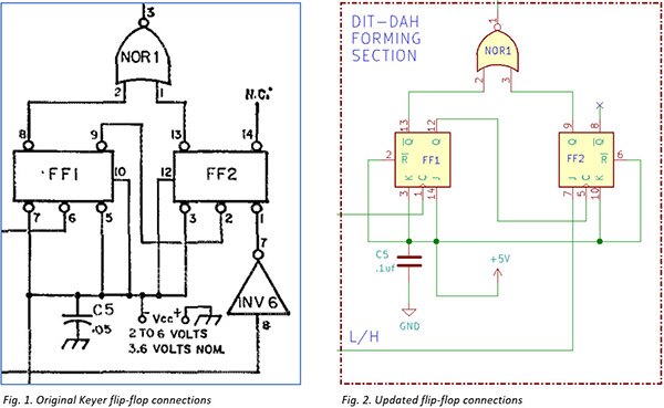
Character Forming is accomplished using two JK flip-flops labeled FF1 and FF2. The obsolete aspect of the MC790P is that it toggles the outputs when triggered and the J and K inputs are held low. The vast majority of modern, readily available flip-flops toggle when J and K are held high, such as Texas Instrument’s CD74HCT73E. The original circuit used a positive chassis ground with the negative supply connected to the J and K inputs (pins 7, 5, and 3). See figure 1. The updated schematic uses a conventional supply configuration with the positive connected to J and K on FF1 and K on FF2. See figure 2.

Other differences between figures 1 and 2 include the reset connections swapped from negative to positive along with the deletion of the inverter (INV 6). The positive signal from the DAH paddle button was previously inverted to facilitate toggling. The new flip-flop requires J on FF2 to be high in order to toggle so the inverter is not needed.
The MC724P Quad 2-Input NOR Gate
Although obsolete, the MC724P is not that much different than devices currently available such as Toshiba Semiconductor’s TC74HC02APF. In general, many modern devices use less current and operate faster, which is helpful if the updated Digi-Keyer remains battery-powered.
It takes three DITs to make a DAH
Before delving into creating characters (DITs and DAHs, aka DOTs and DASHES), the function of NOR1 must be clarified. NOR1 is not only the first stage of the output circuit. It also enables the timing circuit to deliver regular pulses to FF1 for the duration NOR1 output is low. When NOR1 output is high, the pulses cease at the end of the current timing cycle.
The operation of the flip-flops in forming characters is explained using figure 2. Pressing the DIT paddle triggers an initial pulse from the timing circuit that is delivered to FF1 pin 1, which toggles output pins 12 and 13. Pin 13 triggers the output of NOR1, which signals back to the timing circuit that a DIT is in process. At the completion of the timing function, another pulse is sent to FF1 toggling it back to its original state. Note that during DIT formation, FF1 pin 13 is triggering pin 5 of FF2, but because the DAH paddle has not been pressed the output of FF2 remains unchanged. The truth table in the datasheet for Texas Instrument’s CD74HCT73E explains the relationship between the inputs and outputs. Figure 3 outlines the truth table for generating a single DIT.

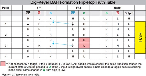
Pressing the DAH paddle also triggers an initial pulse from the timing circuit that is delivered to pin 1 and toggles FF1 output pins, but it also sets J on FF2 high causing the FF2 outputs to toggle as well. As pin 9 of FF2 also triggers NOR1, the output of NOR1 does not change back to its normal state until FF1 and FF2 have both returned to their original state, which requires three DIT cycles. The QST article states that “DAHs override the DITs.” which is demonstrated here. Figure 4 outlines the truth table for generating a single DAH.

The MC789P Hex Inverter
Much like MC724P, the MC789P is obsolete but is not much different than hex inverter ICs currently available such as Texas Instrument’s CD74HC04E which uses less current and is faster, requiring some tweaking of the original keyer RC timing components to take into account propagation delay. Propagation delay is the accumulation of time for a signal to pass through ;multiple devices. Each device slows down the signal a very small amount, but it adds up.
Asynchronous Timing Made to Order
On-board clock generators are a common way to keep a circuit running in perfect harmony. But what if the clock needs to “synch” to human input? What if that input is unpredictable and highly variable like the rapid manipulation of key or paddle contacts by hand? The solution is an asynchronous timing system that responds to random input and then takes over for a predefined period.
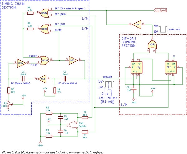
As mentioned earlier, user input causes an initial pulse that starts the Digi-Keyer’s character formation. When the character is complete, another pulse resets the circuit and waits for another user input. Pulses are generated only when needed using inverters and reliable RC timing circuits. Figure 5 includes the entire keyer circuit and shows the relationship between character formation and asynchronous pulse timing.

The output of NOR1 is inverted before it reaches NOR4. A logic high on any input of NOR4 or NOR2 places a logic low at NOR3 indicating a character is in progress, the user is keying a new character, or the pulse space RC circuit is not ready (CLEAR input on NOR2).
A fully charged pulse space RC circuit results in a logic high at INV4 resulting in a low on pin 9 of NOR3. If NOR3’s enable input is also low due to activity, its output goes high causing INV2’s output to go low, which delivers a low transition on pin1 of FF1 causing a start, step, or end in character formation depending upon the current state of the flip-flops.
When INV2’s output goes low, it also provides a ground for the RC pulse width circuit to begin charging. After approximately 8ms, capacitor C2 is fully charged, causing the output of INV2 to be blocked. Now, INV1’s input is held high through R3 causing its output to go low and providing a ground for the RC space width circuit to begin charging and also causing INV4’s output to go high, NOR3’s output to go low and INV2’s output high. When capacitor C1 is fully charged, the output from INV1 is blocked causing INV4’s input high through R1 and R2 and its output low. Now pin 9 of NOR3 is low. If there is still activity, the process begins again. If there is no activity from the user and the current character is complete, the Digi-Keyer waits for the next user input.
Summary
There is logical complexity in this seemingly simple keyer circuit. A builder may also marvel at how a non-microcontroller design accomplishes so much with so few components. It is wise to understand how devices like flip-flops and logic gates can do some heavy lifting can quickly and efficiently leaving the microcontroller for other tasks.
Resources
- Updating the Original Digi-Keyer
- What Are RC Timing Circuits
- Creating Quasi-Sine from Square Waves
- Assembling the Digi-Keyer
- How JK Flip-Flops Work
Interested in building the Digi-Keyer and learning how it works? DigiKey provides the full set of plans, bill of materials, programming code, PCB files, and more in this repository:
https://media.digikey.com/pdf/Project%20Repository/Digikeyer.zip


