Smaller Is Better: Miniaturizing RF - Part 2
投稿人:电子产品
2015-03-12
This article, the second of two parts, examines the miniaturization of some key active components and system elements that will allow designers of next-generation wireless links to provide smaller and more efficient radios and radio subsystems. We will look at small-sized active components like RF transistors, mixers, modulators, and amplifiers and will discuss die-form devices that are useful for System-On-Chip (SOC) and Multi-Chip Module (MCM)-style prototypes and initial production runs.
Part 1 described the latest small-sized passive parts that integrated several discrete parts into smaller surface-mount versions. These save space, cost, and improve performance, and are widely available for use with modern, common standard radio-link transceiver chips whose designs frequently are on their third or fourth generation. Many are usable for next-generation and custom radio design as well.
Active-discrete (or functional-block) components are addressing next-generation radio solutions for Personal Area Networks (PANs) and wearable computers. While not as functionally dense, the flexible parts can be used to continue the trend toward higher-frequency, smaller-wavelength systems. These allow further size reductions and can use lower power levels since the PAN RF field is so limited in volumetric space.
Innovators anxious to lead instead of follow will be designing and building their own next-generation radio systems using presently available building blocks. This article will look at some of these active blocks. All parts, data sheets, reference designs, and development kits referenced in this article can be found online at DigiKey’s website.
Back to square 1–again
When designing next-generation radios, there are two major levels of prototypes typically needed. The functional-development group will want integrated functional blocks with access between the stages for measurement and optimization. This can allow probing and tweaking of values to optimize power transfer and maintain signal integrity on a stage-by-stage basis.
While some advanced radio transceiver chipmakers will manufacture finished product as an MCM, the best return on investment is with a monolithic device. As second- or third-generation devices, the scaled-down monolithic form generally is much more price effective and often smaller and better performing, since it leverages experience gained with earlier versions.
However, this transformation into monolithic form is in effect in a new design. Trace runs on PCBs are typically characterized for tight impedances and transmission-line characteristics. On a Multi-Chip Module or custom silicon die, all characteristics will have to be re-established using the new materials and sizes. So, in effect, it is a new design from a physical perspective.
Here is where RF switches can be so important when prototyping a next-generation radio. By providing switched access to internal nodes, designers can direct signal path, probe, or tune the stage. However, note that the switches need to be tuned as well. Standard contact switches may not work with RF. The high-frequency signals use contact spacing (and even dielectric spacing) as feedthrough capacitors. Therefore, special RF switches (and connectors) are needed.
Several good quality and small-sized monolithic and die-form RF switches are ready to serve “off the shelf” for both internal access to prototype stages or for multi-antenna and shared-path designs. Note these are characterized as having lower- and upper-frequency limitations, as well as insertion losses and spectral plots of frequency isolation. Note also that various topologies exist to provide more signal-path flexibility, especially in circumstances where an individual antenna may serve several frequencies, bandwidths, and protocols. A multiplexer, for example, requires fewer signal traces than discrete switches.
Let’s look at the Peregrine 4259-63 reflective RF switch in a compact (SC70-6) package. It exhibits 50 Ohms from 10 MHz to 3 GHz, and is a SPDT general-purpose RF switch with insertion losses as low as 0.5 dB. A nice feature is the selectable single- or dual-line control allowing precise break-before-make operations.
This part is a member of the supplier’s UltraCMOS Series that use sapphire substrates to provide performance comparable to more costly Silicon Germanium or Gallium Arsenide technologies, while also featuring better power handling and ESD tolerance. Family members include RF switches, mixers, and attenuators.
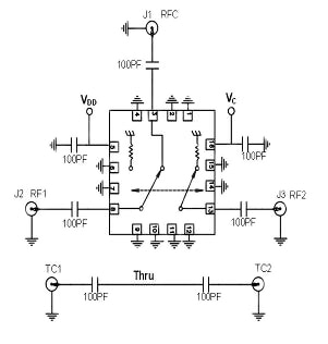
Absorptive types of switches can also be used for mutually exclusive and load-balanced switching. For example, the 50 Ohm SPDT RF3025TR7 from RF Micro Devices features a very wide range from 10 MHz to 6 GHz with a very low 1.1 dB insertion loss (Figure 1). This can become 0.5 dB at frequencies below 1 GHz, providing a clear path for a UHF receiver, for example, sharing the same antenna.

Figure 1: Absorptive switches can feature terminated or loaded non-switched conditions and help maintain consistent signal-path impedances.
Depending on the frequencies of interest, selections of bands range up to 86 MHz operations. For MCM and SoC solutions, an 86 MHz SPDT die RF switch from Hittite (now part of Analog Devices) may do the trick. The HMC-SDD112 features a nice 30 dB isolation frequency at 86 MHz and a fairly low 2 dB insertion loss. While currently for use in modern radar, as more high-frequency and higher-data-rate links are established, additional parts for other applications are bound to become available.
In the mix
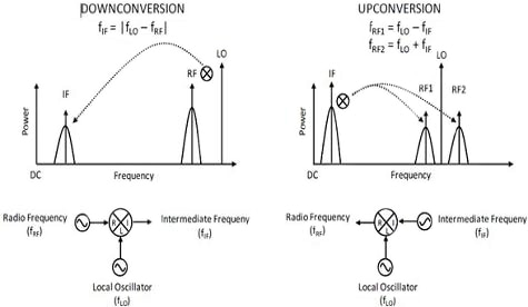
RF mixers are 3-port modulators or demodulators and can be active or passive. They can be used for both up conversion (when used in a transmitter) or down conversion (when used in a receiver) [Figure 2]. The input RF is combined with a local oscillator to create an intermediate frequency that preserves the signals of interest in a mix of initial frequency, local oscillator frequency, and sum and difference frequencies; hopefully without phase shift or attenuation.

Figure 2: Mixers for up conversion (left) and down conversion (right) in both passive and active form provide rudimentary modulation functions needed in radio designs. Active mixers can be part of a next-generation prototype using discrete active components, and migrate on-chip once a monolithic solution is spun.
Passive mixers typically exhibit loss, while active mixers can exhibit gain. While passives can have wide bandwidths and good inter-modulation-distortion characteristics, active mixers can be better integrated onto a single chip solution and can provide both good signal isolation as well as less sensitivity to load matching.
Like switches, mixers are selected for their frequency ranges, losses, and phase characteristics. An example is the Maxim MAX2682EUT+T down converter in a compact SOT23-6 package that can target established ISM and cellular communications designs or implement any new radio designs between 400 MHz and 2.5 GHz. Based on a Silicon Germanium process, it works well for shared GPS and 2.4 GHz ISM links. Maxim provides several App Notes including PCB layout guidelines1, GPS front-ends2 and satellite receiver links3.
Several good choices exist for 5 GHz bands as well, which can share connectivity with 2.4 GHz bands for higher-speed, dual-band wireless LAN connections. Parts like the Hittite HMC557LC4TR can function as both an up converter and down converter in a transceiver design spanning 2.4 GHz to 7 GHz with a wide DC-3 GHz IF bandwidth.
Higher-band 6 GHz to 10 GHz parts like the Hittite HMC520LC4TR are useful for imaging applications such as in wall wire, stud, and nail detectors. Also, for next-generation wearable computers, the HMC1081 will handle the 60 GHz bands now being toyed with for PAN applications. These ultra-small units will require monolithic solutions, so die parts like the HMC1081 are ideal to use on your prototype MCMs.
RF transistors
When external drive is needed to provide more output power than a monolithic transmitter typically can handle, external RF transistors can be used. These parts can be placed closer to the actual antennas to improve efficiency and provide higher transmit current. RF transistors can also be used as higher-power switches to isolate sensitive receive sections while higher-power transmit is taking place.
Often, output drivers use NPN and PNP transistors since they are tougher than FETs (but not always). FETs are very effective at offering the lowest ON resistances and as a result can be used more effectively in the signal path. This can be to direct a signal path, such as to another antenna for example, or to tap into a signal chain for probing purposes. As expected, transistor selection will primarily be based on operational frequency and voltage, but low RDS(ON), current-handling capability, and size are also key factors.
Transistors can be used in all bands, including UHF, which has advantages when signal penetration through walls and structures is important. Parts like the CEL NE68019-A support sub-2GHz signals in a compact 3-pin SOT 543 and can provide higher output power than typically available inside a monolithic radio chip.
The Toshiba 2SC5084-O(TE85L,F) can also be used, which is good up to 7 GHz with 150 mW of output-power-handling capability. This can easily handle 5 GHz so it can be used with dual-band Wi-Fi as well as ZigBee, GSM, Bluetooth, and other 2.4 GHz protocols.
Lower-frequency parts like the 50 Ohm input-and-output Toshiba 2SC2714-O(TE85L,F) can be used for FM-output stages as well as IF switching with higher-frequency mixers. Selectable IF oscillators can allow the same transceiver blocks to handle different bandwidths. Note also that transistor arrays can be used as well to save even more space, but you may lose the layout advantages of placing single elements wherever you want.
Die products
A wide variety of die product are available for MCM prototypes or pilot runs. With flash-annealed-ceramic substrates, even passive SMT devices can coexist with die-bonded devices. In addition, chip-on-board technology can be used with RF stackups to incorporate board and/or chip antennas.
The many discrete functions, such as attenuators, amplifiers, mixers, and modulators, provide a lot of freedom when structuring a new radio design. What’s more, they provide the highest level of functional integration with the least risk since each functional block is well characterized and working right out of the chute.
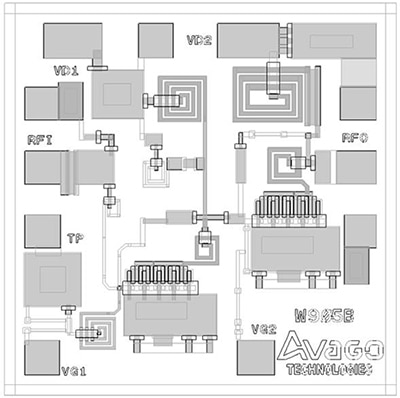
Whether it’s a 6-20 GHz 3-stage amplifier like the Avago AMMC-5618-W10 (Figure 3) or a 20 Watt 8-10.5 GHz PIN-diode terminated SPDT switch like the MA/Com MASW-010647-13950G, all the pieces are there to pioneer upcoming standards.

Figure 3: Note the complexity of even simple functions like this 20 GHz-amplifier die layout. Using active die and passive arrays for prototypes provide dense and efficient MCM designs using known building blocks.
Some unusual parts are also available like the 2X frequency multiplier for 20-40 GHz operation. The Avago die packaged AMMC-6140-W10 has a 50 Ohm input and output impedance while providing a linear-frequency doubling.
Another interesting option is the ATN3590-10 attenuator pad from Skyworks Solutions.
These fixed-resistive attenuators are ideal for coplanar waveguides or micro-strip circuit carriers. Available with fixed-attenuation steps, these can allow stepped-level adjustments when combined with reflective-RF switches.
In summary
Most of us will be using integrated chipsets from major suppliers once a protocol and the link characteristics become a widely accepted standard. Successive generations will provide free software stacks and make radio design more of a cut-and-paste operation.
However, for those pushing the digital-radio envelope, miniaturization remains one of the key driving factors – especially for such high-growth applications as wearable computers and peripherals.
For more information about the parts discussed in this article, use the links provided to access product pages on the DigiKey website.
References
免责声明:各个作者和/或论坛参与者在本网站发表的观点、看法和意见不代表 DigiKey 的观点、看法和意见,也不代表 DigiKey 官方政策。


 中国
中国