New Buck-Boost DC/DC Converters Offer Jitter-Free Transition with High Efficiency
投稿人:电子产品
2015-08-11
There are many industrial and automotive applications where input voltages can vary over a wide range. Similarly, battery-powered consumer products also experience large changes in the input voltages of their converters. Under such conditions, a DC/DC converter must deliver the regulated output voltage even when the input voltage is below, above, or close to the required load voltage. A buck-boost DC/DC converter addresses such needs. Over the years, suppliers like Intersil, Linear Technology, and Texas Instruments, among others, have offered myriad low-noise, high-performance, wide-input buck-boost DC/DC converters that have adequately served these needs (see the TechZone article “Buck-Boost DC/DC Handles Wide Input-Voltage Range”).
Now these suppliers have readied a new generation of buck-boost DC/DC converters with many novel features and functions, including jitter-free transition between buck and boost modes. In addition, they deliver high-load current with high-conversion efficiency from a wide range of power sources. Linear has recently released LTC3118, a new dual-input, wide-voltage-range synchronous buck-boost DC/DC converter with an intelligent, integrated low-loss PowerPath control. What’s more, for higher load current and single input, it has readied a new buck-boost µModule (micromodule) regulator with higher input voltage capability, the LTM8056.
Similarly, Intersil has released highly integrated buck-boost switching regulators, designated ISL91108 and ISL91110, that offer high efficiency across wide load variations due to its fully synchronous 4-switch architecture.
This article will explore these new buck-boost DC/DC converters in detail, investigating their novel architectures that deliver high efficiency across light-load to full-load with lower quiescent current. In addition, application circuits will be presented to demonstrate ease of use and performance in end applications and products.
New generation buck-boost
According to Linear, the need to operate from multiple input sources is common for applications powered by various battery chemistries, wall adapters, and DC voltage rails like USB. Consequently, the dual-input capability of LTC3118 makes it suitable for applications that use batteries or supercaps as secondary or backup inputs, in case the traditional primary input is interrupted. Likewise, applications that use multiple sources such as a wall adapter and Lithium-ion (Liion) cells can also utilize the dual input feature of the new buckboost DC/DC converter.
While this looks simple and straightforward, in reality it is not. According to the LT Journal of Analog Innovation article1 “18 V Buck-Boost Converter with Intelligent PowerPath Control Delivers >2 A at 95% Efficiency from Dual Inputs” by Eddy Wells, losses in the power path, prioritization of the input sources, and voltage spikes from inductive cable insertion can contribute to the cost and complexity of the system. As per Wells’ explanation, the LTC3118 addresses these issues by combining a dual, low loss PowerPath controller with a high-efficiency buck-boost converter, as shown in Figure 1.
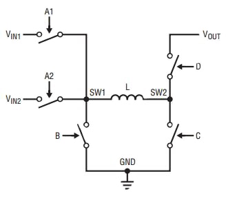
Figure 1: LTC3118’s unique dual-switch architecture allows conversion from either input source, VIN1 or VIN2, to a regulated output voltage VOUT, which can be above or below either input. (Courtesy of Linear Technology)
This novel dual-switch architecture allows conversion from either input source, VIN1 or VIN2, to a regulated output voltage, VOUT, which can be above or below either input. Operation up to 18 V provides sufficient voltage margin for 12 V nominal supplies. Transitions between the step-up or step-down operating modes are seamless and free of transients, making it suitable for noise-sensitive applications, says Linear.
For applications requiring high current, the buck-boost converter can deliver up to 2 A of continuous output current from a wide range of power sources, including single- or multiple-cell batteries, supercapacitor stacks, and wall adapters. Its 2.2 V to 18 V input range on both the inputs and 2.0 V to 18 V output range can provide a regulated output with inputs above, below, or equal to the regulated output.
The LTC3118 uses a low-noise, current-mode control architecture to respond rapidly to line or load transients, as well as maintain tight regulation at the output. The intelligent PowerPath controller plus a single inductor buck-boost converter are integrated in a 4 mm × 5 mm QFN or 28-pin TSSOP package. For an optimal trade-off between switching losses and external component size, the converter operates at a fixed-switching frequency of 1.2 MHz. System-level features include ideal diode or VIN priority modes, VIN and VOUT power-good indicators, accurate RUN comparators to program independent under voltage lockout (UVLO) thresholds, and output disconnect in shutdown. Other features include 2 µA shutdown current, short-circuit protection, soft-start, current limit, and thermal-overload protection.
The LT Journal article in Ref.1 provides a complete application circuit based on LTC3118, which is depicted in Figure 2. In this application circuit, as per the reference, a 2-cell Li-ion battery is placed on VIN1 and a 12 V wall-adapter is placed on VIN2.
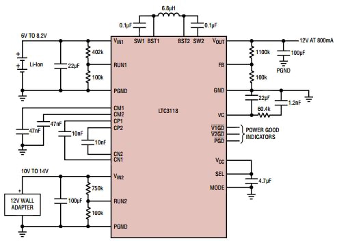
Figure 2: A dual-input application circuit using buck-boost converter LTC3118. (Courtesy of Linear Technology)
In this example, ideal diode mode is selected to ensure operation from the 12 V adapter when it is present. As shown in Figure 3, high efficiency is achieved over a wide-load range from either input source. Additionally, it shows that Burst mode operation facilitates high efficiency at light loads from either source. In this application circuit, the battery is placed on VIN1 because it has lower RDS(on) MOSFETs and is able to support slightly more load current at low VIN in step-up mode. As per this reference, maximum load current for this circuit is 800 mA when driven from the low end of the battery’s voltage range, which is 6 V.
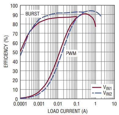
Figure 3: LTC3118 offers high efficiency over a wide-load range from either input source. (Courtesy of Linear Technology)
A few more applications are presented in Ref. 1, suggesting that LTC3118 offers designers maximum system flexibility in dual-input designs.
Integrated solutions
For higher load current and single input, Linear has readied a new buck-boost µModule (micromodule) regulator with higher input voltage capability. With a wide-input voltage range of 5 V to 58 V, the LTM8056 also offers wide-output voltage range with adjustable input and output average current limits. It is housed in a compact BGA package to provide a precisely regulated output voltage programmable via an external resistor divider from 1.2 V to 48 V with 4 A load. The BGA package includes switching buck-boost controller, power switches, inductor, and support components (Figure 4). Selectable switching frequency range is 100 kHz to 800 kHz with easy synchronization using SYNC input and CLKOUT output pins.
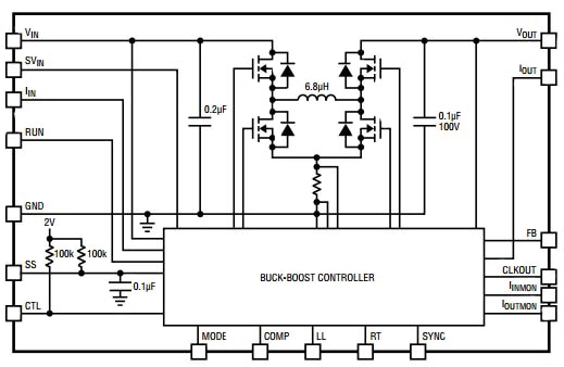
Figure 4: Buck-boost µModule regulator LTM8056 supports higher-input voltage up to 58 V with 4 A load. It comes in a compact BGA package, which includes a switching controller, power switches, inductor, and support components. (Courtesy of Linear Technology)
Likewise, Intersil has also released new integrated switching buck-boost regulators, ISL91108 and ISL91110, with seamless transition between operating modes without significant output disturbance. They provide excellent efficiency across wide-load variations due to the use of fully synchronous 4-switch architecture (Figure 5). No-load quiescent current is only 27.5 μA for the ISL91108 unit, which optimizes efficiency under light-load conditions. According to the product data sheet, forced PWM and/or synchronization to an external clock may also be selected for noise-sensitive applications.
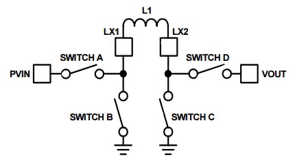
Figure 5: Intersil’s newest buck-boost regulators incorporate fully synchronous 4-switch architecture to deliver high efficiency across wide-load variations. (Courtesy of Intersil)
To keep power supply solutions small, the buck-boost regulators, ISL91108 and ISL91110, switch at 2.5 MHz. The units are packaged in advanced wafer-level CSP packages to reduce the footprint of the device. Furthermore, the switching buck-boost regulators require only a single inductor and very few external components to complete the solution (Figure 6).
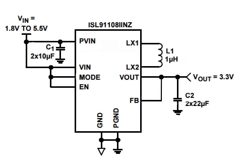
Figure 6: A typical fixed-output application circuit for ISL91108 indicates that only an inductor and a few external components are needed to complete the solution. (Courtesy of Intersil)
With output current of up to 2 A at 3.3 V, ISL91110 is the highest-current switching regulator of the series with an input as low as 2.5 V. Its quiescent current is 35 µA. Similarly, ISL91108 is rated for 1.6 A at 3.3 V with an input as low as 2.8 V. Its quiescent current is only 27.5 µA.
In summary, the new-generation buck-boost converters bring many novel features and functions to address a wider range of applications. Besides offering jitter-free transition between buck and boost modes, they are also delivering high-load current with high-conversion efficiency from a wide range of power sources. In addition, the input-voltage range is widening as is the output.
For more information on the products discussed in this article, use the links provided to access product pages on the DigiKey website.
References
- “18V Buck-Boost Converter with Intelligent PowerPath Control Delivers >2A at 95% Efficiency from Dual Inputs” by Eddy Wells, LT Journal of Analog Innovation, April 2015.
免责声明:各个作者和/或论坛参与者在本网站发表的观点、看法和意见不代表 DigiKey 的观点、看法和意见,也不代表 DigiKey 官方政策。


