Buck-Boost DC/DC Handles Wide Input-Voltage Range
投稿人:电子产品
2013-07-30
A buck-boost DC/DC converter delivers a regulated output voltage even when the input voltage is below or above that required by the load. Buck-boost converters adequately serve the needs of battery-powered consumer devices where the required input range is rather narrow; in many cases from 1.8 to 5.5 VDC. However, the situation is different when it comes to industrial and automotive applications where input voltages can vary over a very wide range.
For example, the automotive battery presents one of the most challenging inputs to a power supply. While its nominal voltage can vary from 10.6 to 15 V, depending on the battery’s state of charge, the ambient temperature, and the alternator, cold-crank conditions can push the rail below 4 V and line transients can produce 40 V spikes. That means it can vary from less than 4 V to over 40 V. In addition, experts say that the automotive power rail is also subject to a variety of dynamic disturbances produced by changes in the engine, transitioning loads, and inductive transients in the wiring harness.
To address the needs of industrial and automotive applications, power semiconductor suppliers such as Intersil, Linear Technology, and Texas Instruments, among others, have developed a variety of low-noise, high-performance, wide-input buck-boost DC/DC converters. As a result, a variety of products are available that can help power designers confront the challenges of generating a stable output voltage using a single low-cost inductor, despite very wide fluctuations in the input voltage range.
Buck-boost regulator
Ensuring seamless transition between operational modes, Linear’s synchronous buck-boost converter LTC3115-1 uses a proprietary low-noise switching algorithm to deliver stable output voltage with high efficiency while input voltage can go above, below, or be equal to the output voltage over a very wide range. The specified input range for this part is 2.7 to 40 V. Switching frequencies up to 2 MHz are supported to allow the use of small-value inductors for miniaturization of the application circuit.
According to Linear, for automotive electronics the LTC3115-1 (Figure 1) provides uninterrupted operation through load dump transients and even in the harshest cold-crank conditions. Plus, its programmable high switching frequency, in conjunction with a low-noise PWM control algorithm, keeps switching noise and harmonics above the AM broadcast band with minimal electromagnetic (EMI) emissions under all operating conditions and modes. In addition, an internal phase-locked loop (PLL) allows switching edges to be synchronized with an external clock for further control of EMI in noise-sensitive applications.1
Figure 1 shows a 5 V automotive supply for use in engine control units and for other critical functions including safety, fuel system, and drive train subsystems, where processors must remain powered without fail during the most severe input voltage transients. This application circuit can use up to 2 MHz switching frequency to minimize footprint and eliminate interference with the AM broadcast band. The VCC rail provides power to the internal circuitry of the LTC3115-1 including the power device gate drivers and is ordinarily powered from the input rail via an internal linear regulator. In this application, diode D1 bypasses the internal linear regulator and delivers power to the VCC rail directly from the regulated output to improve efficiency and output current capability. This is particularly advantageous in applications with higher switching frequencies, given that the increased gate drive current is provided more efficiently from the converter’s output rail than through the internal linear regulator.
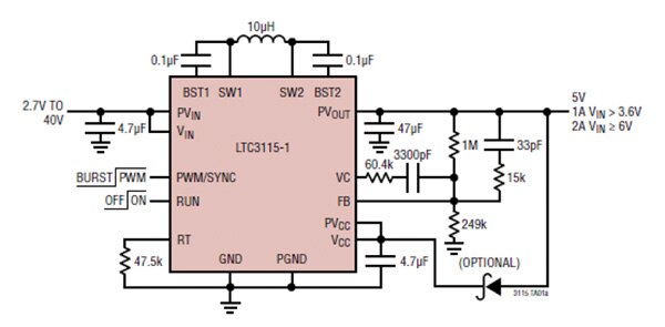
The appropriate selection of external passive components, dependent upon the required performance of the DC/DC and trade-offs such as PCB area, cost, output, and input voltage, allowable ripple voltage, efficiency and thermal considerations is discussed in the datasheet.2 It provides some basic guidelines and considerations in selecting the external components, including the inductor, and the design of the application circuit. In fact, based on thorough examination of the inductor, VCC bypass capacitor, and input and output filter capacitors, Linear Technology recommends component values with part numbers and supplier names.
What is more, the buck-boost converter can be operated in the burst mode to reduce standby current and improve light load efficiency. The burst mode is pin selectable. Other features include output disconnect in shutdown, short-circuit protection, and internal soft-start. The LTC3115-1 is available in thermally enhanced 16-lead, 4 mm × 5 mm × 0.75 mm DFN and 20‑lead TSSOP packages.
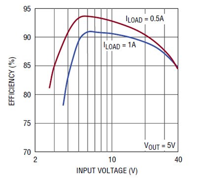
The efficiency performance for the application circuit in Figure 1 for load currents of 500 mA and 1 A with 3.3 to 40 V input voltage range is depicted in Figure 2. It shows that when the input is close to the output, the circuit offers high efficiency, close to 93 percent for a load of 500 mA. Efficiency remains over 90 percent for a load of 1 A. At the same time for voltages as low as 3 V and as high as 40 V, the LTC3115-1-based DC/DC converter circuit maintains an efficiency of over 85 percent.
Given that for industrial applications typical voltages required are 12 V and 24 V DC, Linear also provides values for external components for LTC3115-1-based DC/DC converter circuits with 12 and 24 V outputs. The measured efficiency performance for these circuits is presented in the datasheet (again, see Reference 2).
Ultra-wide input
For applications that require an even wider input voltage range, Texas Instruments has readied an automotive-grade buck-boost regulator with integrated MOSFETs for voltage-mode control. Incorporating all the functions required to implement a high-performance, cost-efficient buck-boost DC/DC converter, the TPS55065 regulates output to 5 V ±3 percent for an input voltage range of 1.5 to 40 V. A typical application circuit with passive component values for a 5 V regulated output is illustrated in Figure 3. While the selection of passive component values are system dependent, the manufacturer recommends using low-ESR capacitors on the output to minimize voltage ripple on the output due to transients. Also, the external inductor for the switch-mode regulator, connected between terminals L1 and L2, must be placed close to the terminals to minimize parasitic effects.
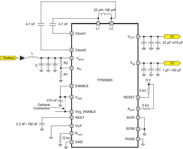
For stability, TI recommends an inductor with inductance of 20 to 100 µH, as shown. Also, a low-EMI inductor with a ferrite-type closed core is preferred over other types, and it must be located away from low-power traces and components in the circuit. In addition, the DC/DC converter’s datasheet3 suggests keeping input ceramic filter capacitors in close proximity of the VDRIVER terminal and using surface-mount capacitors to minimize lead length for reduced noise coupling. Likewise, all power (high-current) traces should be thick and as short as possible for reduced EMI.
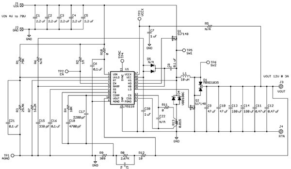
If the application demands even wider input range, TI has developed a buck-boost switching regulator controller, designated LM5118 that can handle an input range of 3 to 75 V. It integrates high- and low-side MOSFET drivers capable of supplying peak currents of 2 A. The regulator control method is based on current mode control using an emulated current ramp. The operating frequency is user programmable from 50 to 500 kHz. To evaluate the LM5118 controller IC, TI offers an evaluation board4 that is designed to provide the design engineer with a fully functional, emulated current-mode control, buck-boost power converter. The evaluation board (Figure 4) provides a 12 V output with 3 A of output-current capability. Its wide input voltage range is from 75 to 5 V, with operation down to 3 V with some component changes.
In summary, to address applications ranging from battery-operated consumer devices to automotive and industrial systems, buck-boost DC/DC converters today deliver high-performance regulated output with both narrow and wide input voltage fluctuations. For more information on the parts discussed in this article, use the links provided to access product pages on the DigiKey website.
References
- “2.7V to 40V Monolithic Buck-Boost DC/DC Expands Input Capabilities, Regulates Seamlessly through Automotive Cold Crank and Load-Dump Transients”, John Canfield, LT Journal of Analog Innovation, January 2013
- Datasheet: Linear Technology LTC3115-1
- Datasheet: TI TPS55065
- TI User’s Guide for AN-1819, the LM5118 Evaluation Board
免责声明:各个作者和/或论坛参与者在本网站发表的观点、看法和意见不代表 DigiKey 的观点、看法和意见,也不代表 DigiKey 官方政策。
