Taming the Large-Screen Tablet: A Cost-Effective Way to Simplify Capacitive Touchscreen Controls
投稿人:DigiKey
2012-01-11
Here's a question – what do Apple, Samsung, Motorola, RIM (the maker of the Blackberry), Asus, Acer, and HTC have in common? They all have competing capacitive touchscreen tablets in the consumer market. Seeing the enormous success of Apple's iPad, companies are racing to enter the market and looking for ways to differentiate through industrial design, the software interface, hardware specs, or price.
The capacitive touchscreen assembly is one of the most expensive components in a tablet, and also one of the areas where companies are trying to differentiate. Apple set a size standard of 9.7 inches, while Samsung and Motorola attempted variations of 7 inches and 10.1 inches. Also, when Windows 8 arrives, there are likely to be versions designed as laptop replacements that use screens as big as 14.1 or 15.6 inches. Transitioning from a smaller capacitive touchscreen to a larger one, while at the same time trying to maintain a similar level of touch sensitivity and performance, can pose several challenges. There are the usual issues of power consumption, PCB size, and weight, but performance and price also have to be taken into account. Since the touchscreen assembly is a big-ticket item, any cost savings in its production can have a direct impact on retail pricing and margin. The screen needs to be responsive and accurate, but manufacturing costs need to be kept in check.
Of the various components that make up a touchscreen assembly, two correlated items give engineers the greatest opportunity to influence the price/performance ratio. First, there is the design and implementation of the Indium-Tin Oxide (ITO) pattern, which presents a change in surface capacitance when the screen is touched by a fingertip. Second, there is the configuration of the control circuitry, which is used to translate the capacitance variations into data, indicating location and gesture, which is used by the system's application processor. The ITO pattern has an impact on the number of ICs used in the control circuitry, so it is important to consider them in tandem.
In this article, we take a closer look at these two factors, and suggest an approach that is both scalable and cost-effective. We begin by looking at tradeoffs associated with the ITO pattern, and then evaluate options for implementing the control circuitry.
The ITO pattern
Figure 1 shows the ITO pattern of a typical capacitive touchscreen measuring at least 7 inches.

The control circuitry
For the sake of simplicity, cost, and time-to-market, early entrants in the tablet market used capacitive touchscreen solutions that were originally designed for mobile phones. Now, as engineers begin incorporating larger screens, they are finding it difficult to continue using the same control ICs. This is because the larger screens require more general-purpose I/O (GPIO) and generate more LCD noise.
Increases in GPIO
In a typical implementation that uses mutual capacitance, the number of GPIO required for touchscreen control equals the sum of the X and Y ITO sensors. For example, a touchscreen sensor IC with 32 GPIO can support a screen measuring 5 inches and with a relatively dense ITO pattern of 20 X sensors and 12 Y sensors. The same sensor IC can be used with a 7-inch WSVGA display (1024 x 600), but there may be a reduction in accuracy and responsiveness, since the 20 x 12 grid needs to use larger ITO cells to cover the increased area. With a 10.1-inch display (1280 x 800), the situation worsens. To achieve the same level of touch sensitivity and resolution as in the 5-inch display with 32 sensors, the touchscreen sensor IC will need more than 50 GPIO. For this reason, a 7-inch screen is typically the "size ceiling" for a tablet that uses a single-chip controller originally designed for a smartphone. Beyond 7 inches, the engineer usually needs more than one sensor IC. This break-off point is generally used to categorize screens, with assemblies in excess of 7 inches being referred to as "large-size" touchscreens.
Increases in LCD noise
LCD noise is another problem when using a legacy sensor IC with a newer, larger screen. Today's LCD technologies, which are designed for faster switching and higher brightness, also emit a high degree of interference. In a screen of less than 5 inches, the touchscreen controller can typically use a 5 V DC input signal applied to the ITO traces (with proper tuning and impedance matching), to achieve a good signal-to-noise (SNR) ratio. However, when the screen size increases to more than 7 inches, a DC voltage of 10 to 15 V is usually necessary for improving the SNR. The legacy sensor IC may not be able to drive above 10 V DC without using external passive components, which take up space and add to the overall cost.
Today’s multi-sensor approach
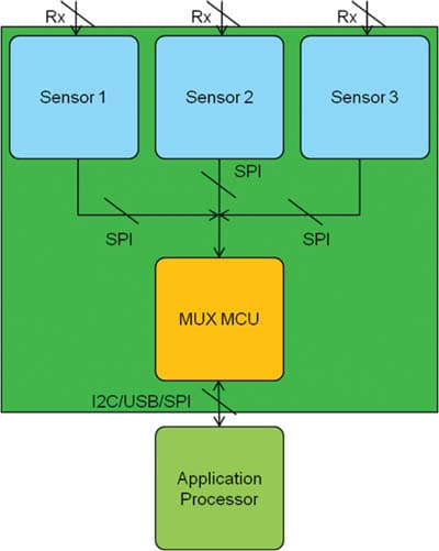
To avoid these GPIO and noise problems, engineers often use a multi-sensor "divide and conquer" approach. The touchscreen is divided into several virtual sections, different touch sensors are used to cover each section. The various sensors are grouped together to represent the capacitive touch sensing of the entire screen. Figure 2 gives a sample illustration. The three touch sensors provide inputs to a general-purpose "mux" microcontroller with a multi-channel SPI interface, which in turn transfers finger-position data to the system application processor for software manipulation.

In this approach, the touch sensors perform the analog processing required to project variations in capacitance, while the mux MCU, which has a higher CPU clock, performs the processing necessary to identify finger coordinates, timing, and gesture.
Solutions based on the multi-sensor approach are readily available from several leading vendors, but these off-the-shelf solutions can pose two distinct disadvantages. First, the increased number of components usually means a bigger footprint for the touchscreen controller circuitry, and that can increase cost. Second, these solutions typically use a proprietary algorithm for analog and digital processing, which often means carrying a higher price tag and presenting a certain amount of risk when it comes to supply management.
The evolving ASIC approach
In response to the current disadvantages of today's multi-sensor approach, new methods are beginning to emerge. One evolving approach uses a single-chip touch sensor, specially designed to support a large-size touchscreen, in combination with an inexpensive, general-purpose MCU.
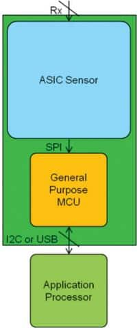
There are several IC design houses working on single-chip sensors for touchscreens. These custom-designed sensors have lots of pins for driving the ITO grid, and they can even be made to output a higher-voltage DC signal (15 to 20 V), to lessen the impact of LCD noise. The result is higher touch resolution and sensitivity thanks to the increased number of ITO channels and the improved SNR. Figure 3 illustrates this ASIC approach. Only one ASIC touch sensor is required for processing the analog signals for the entire panel, and the system replaces the higher-priced mux MCU used in the multi-sensor approach with an inexpensive, general-purpose MCU.

The cost difference between the multi-sensor system in Figure 2, which uses three touch sensors and one mux MCU, and the ASIC system in Figure 3, with its single touch sensor and general-purpose MCU, can be as much as two or three dollars. In terms of the overall cost of the touchscreen assembly, this can represent significant savings.
Also, with the ASIC approach, the software algorithms for touchscreen control can be developed and managed in-house. Being able to integrate the software IP and the hardware components reduces the system costs further and creates a competitive advantage.
Selecting an MCU for the ASIC approach
Engineers who use the ASIC approach can choose from a variety of general-purpose MCUs. Since the microcontroller only communicates with one input device (the ASIC touch sensor), it no longer needs to multiplex the input signals, and that makes for a simpler firmware and timing arrangement. Table 1 gives the selection criteria for a general-purpose MCU to be used with a 10.1-inch touchscreen.
| Feature | Requirements | Comments |
| CPU clock | 40-50 MHz | |
| SRAM | 8 KB | |
| Flash | 32 KB | |
| SPI | Yes, > 15 MHz | Master and slave modes |
| I²C | Yes, > 400 kHz | Potentially long PCB trace between MCU and application processor |
| USB | Yes*, Full-Speed USB required | *Only for a Windows-based tablet; must also support remote wake-up and selective suspend |
| GPIO | 3-5 additional | Additional GPIO for dedicated system features |
In addition to the hardware requirements listed in Table 1, there are a few other things engineers should keep in mind:
- CPU clock – A typical 8-bit MCU cannot support a CPU clock of more than 30 MHz. A 40 to 50 MHz CPU clock requirement means that a 16- or 32-bit MCU should be used.
- I²C and/or USB interface – I²C is the interface typically used between the MCU and the application processor. However, Windows operating systems use USB for input peripherals. Choosing an MCU that has both I²C and Full-Speed USB lets the platform support both Android and Windows, but the additional USB interface can increase cost.
- Package – In mobile electronics, a smaller footprint is always preferred. The best choices to look for are QFN, BGA, and Chip-Scale Package (CSP).
- Power consumption – Lower average power means longer battery life. Given the higher CPU clock requirement, finding an MCU with a good power/performance ratio is key.
- Scalability – Ideally, the MCU has a pin-compatible “cousin” that supports even faster CPU speeds and bigger Flash memories, so the same MCU architecture can be used with even larger screens.
- Peripheral performance – The MCU's SPI interface has to be fast enough to work with the sensor ASIC, which transfers the analog signal from the entire panel all at once. Also, the touchscreen circuitry is often implemented on a separate PCB, close to the touchscreen, so the ASIC and MCU may end up being far away from the applications processor, which resides on the system's main board. That means it is important to find an MCU with an I²C interface robust enough to reach the application processor.
After evaluating the above criteria, many engineers choose an ARM-based Cortex-M0 microcontroller. The Cortex-M0 architecture delivers low power at a low cost, and offers superior code density with an excellent power/performance ratio. Cortex-M0 MCUs have the peripherals and interfaces required for touchscreen applications, and designs based on Cortex-M0 can easily be scaled up to the higher-performing Cortex-M3 architecture for use with an even larger screen.
NXP Semiconductors offers several options for ARM Cortex-M0 in touchscreens. In particular, the LPC1100L series operates at up to 50 MHz, has up to 32 KB of Flash, 8 KB of SRAM, a high-speed SPI interface (up to 25 MHz), and an I²C interface with ten times the bus-drive capabilities of a typical Fast-mode I²C interface. LPC1100L devices are available in small QFN33 packages, and extend battery life with low power consumption. Active current is only 130 µA/MHz, and deep-sleep current is rated at just 2 µA. The series builds on the LPC1100L series by adding an extra SPI interface and a Full-Speed USB interface. Developers of large-size touchscreens can use the LPC11U00 series to create a single platform that supports multiple operating systems.
Conclusion
As iPad-like tablets continue to gain widespread acceptance among consumers, companies are rushing to deliver tablets with larger, brighter, more responsive capacitive touchscreens. As a result, engineers are looking for ways to improve performance without a spike in costs. Until there is a true single-chip solution for controlling large-scale touchscreens, one approach, which combines an ASIC touch sensor with a general-purpose MCU, provides a scalable, cost-effective interim solution. NXP's LPC1100L and LPC11U00 series of ARM-based Cortex-M0 microcontrollers provide the right combination of features to support the ASIC approach, and help engineers deliver tablets with large-size touchscreens as quickly as the market demands.

免责声明:各个作者和/或论坛参与者在本网站发表的观点、看法和意见不代表 DigiKey 的观点、看法和意见,也不代表 DigiKey 官方政策。


 中国
中国