Pay Attention to the ADC Precision Voltage Reference for Accurate IoT Sensing
投稿人:DigiKey 北美编辑
2016-06-17
The latest analog-to-digital converters (ADC) offer high-performance signal conversion for a wide range of application requirements. For Internet of Things (IoT) designers, a key issue remains one of balancing requirements for precision measurement against the desire to minimize design size and complexity. In reaching for this balance, designers face a key decision in adopting the most effective voltage reference source for their application. Voltage references integrated into ADCs help simplify design, but when the application requires optimal measurement accuracy, external voltage reference ICs are typically the clear choice.
Accurate measurement is fundamental to an IoT vision of detailed analysis of physical phenomena, and precision voltage references are essential for accurate measurement. Regardless of an ADC's underlying architecture, its operation fundamentally relies on the comparison of an input voltage to a reference voltage to create an appropriate output code based on those values. In an ideal case, this relationship is expressed as:
Output code = VIN x (2n/VREF)
where:
VIN is the analog input voltage to the ADC,
n is the number of ADC output bits, and
VREF is the analog value of the reference voltage supplied to the ADC.
Traditional voltage reference designs are built around a bandgap reference circuit (Figure 1). In this conventional design, the output is produced by summing voltage components with opposite polarity temperature coefficients to produce an output voltage that is reasonably temperature-stable and equal to the silicon bandgap voltage of 1.205 V. Most voltage reference designs extend this basic design with circuitry to increase the reference voltage level and buffer the output against load changes.
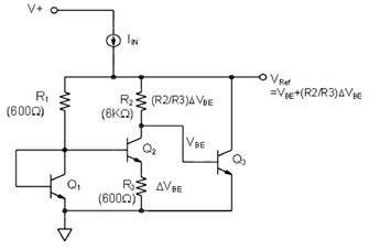
Figure 1: A traditional bandgap voltage reference circuit sums ΔVBE and VBE components, which have temperature coefficients of opposite polarity, to generate a stable voltage equal to the silicon bandgap voltage of 1.205 V. (Source: Analog Devices Inc.)
Reducing noise
Linear Technology uses an alternate approach with its LT1027 voltage reference IC, which is based on Linear's proprietary advanced subsurface Zener bipolar process. With their unique breakdown-voltage characteristics, Zener diodes seem ideal for use in voltage reference designs, but imperfections and contaminants degrade the performance of Zener diodes that are fabricated on surface layers of semiconductor die. In contrast, buried structures combine the advantages of Zener breakdown characteristics with improved noise and stability. Using this low-noise approach, the LT1027 provides a highly flexible precision reference IC for use with high-resolution ADCs such as the Linear Technology LTC2345-16 – a low noise 8-channel simultaneous sampling successive approximation register (SAR) 16-bit ADC with differential, wide, common-mode range inputs.
Although manufacturers continue to work toward minimizing noise, the active circuits in any semiconductor device will generate noise voltage in the 1/f region and the broadband region. Data sheets for voltage references typically include specifications for output-voltage noise over the frequency range of 0.1 to 10 Hz, which encompasses the 1/f region. Semiconductor manufacturers sometimes also include specifications for noise in the broadband region. For its LT1027 voltage reference, Linear Tech provides noise specifications in both regions: In the 0.1 Hz ≤ f ≤ 10 Hz 1/f region, the device produces 3 μVP-P; in the broadband frequency range from 10 Hz to 1 kHz, it exhibits 2.0 (typ) and 6.0 (max) μVRMS.
Because maximum conversion accuracy requires minimum noise levels, designers will often incorporate different methods to reduce noise. In one common approach, designers limit broadband noise by adding a low-pass filter with an extremely low corner frequency at the output of the reference. Voltage reference IC manufacturers also offer different options for lowering noise. With the LT1027, designers can further reduce noise by taking advantage of the device's Noise Reduction (NR) pin, which brings out the positive input of the internal scaling amplifier (Figure 2). By connecting a 1 μF mylar capacitor between the NR pin and ground, designers can reduce the wideband noise of the LT1027LS8 from 2.0 μVRMS to approximately 1.2 μVRMS in a 10 Hz to 1 kHz bandwidth without affecting the device's transient response.
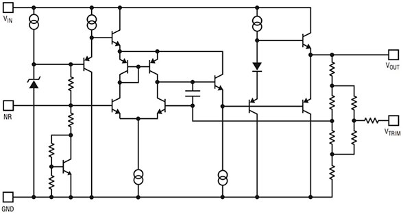
Figure 2: Based on a buried Zener design, the Linear Technology LT1027 voltage reference IC includes a noise reduction (NR) pin that allows further reduction in broadband noise in the output voltage. The device's VTRIM pin enables designers to adjust output voltage. (Source: Linear Technology)
Still, use of this noise-reduction approach requires particular care. Linear Tech emphasizes that electrolytic capacitors are not suitable for this use – the capacitor must be a low-leakage type. A leakage current of just 100 nA will significantly erode performance, resulting in a 150-ppm error in output voltage. Furthermore, Linear Tech calls the NR pin the most sensitive pin on the device and even recommends use of a guard ring in board designs using this approach.
For its ADR440, Analog Devices Inc. (ADI) uses its own proprietary XFET (eXtra implanted junction FET) and temperature correction technologies to reduce noise and enhance stability. According to ADI, XFET is significantly more stable than traditional bandgap references and requires less correction. In turn, these characteristics translate to lower overall noise because they reduce the need for complex temperature compensation circuitry, which is often a major source of noise in bandgap references. This combination of factors results in a very low noise precision voltage reference IC: Analog's ADR440 exhibits only 1 μV p-p in the 0.1 Hz to 10 Hz 1/f region.
In fact, temperature-dependent performance is a significant issue for voltage references, which can be found to be responsible for a large portion of the temperature drift error budget in many systems. For example, a 12-bit system designed to operate over a temperature range from 25°C to 65°C requires that the temperature coefficient of the reference must be no worse than 6 ppm/°C if it is to contribute less than 1 LSB error (Figure 3). Advanced voltage reference devices are designed specifically to ensure temperature stability required for high-resolution ADC systems. For example, the ADR440 exhibits 10 ppm/°C (A Grade) down to 3 ppm/°C (B Grade), while the LT1027LS8 achieves 2 (typ) and 5 (max) ppm/°C.
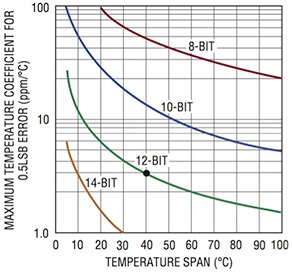
Figure 3: As ADC resolution increases, a voltage reference needs to provide a correspondingly lower temperature coefficient to maintain a 0.5-LSB (least significant bit) error level. (Source: Linear Technology)
Buffered output
Even using a voltage reference device with optimal characteristics for noise and temperature, designers can find that apparent errors arise during conversion, particularly at higher rates. During the normal execution of the conversion process, an ADC will draw different amounts of current from the reference source (Figure 4). In turn, the designer must ensure that the voltage reference source remains unaffected by changes in load.
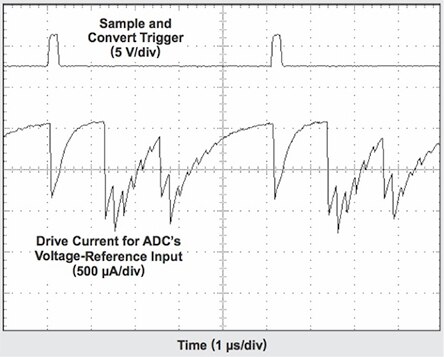
Figure 4: Each conversion cycle (top trace) of an ADC results in varying drive-current demand on the voltage reference, dictating a need for a precision op amp and a capacitor at the output. (Source: Texas Instruments)
To maintain a stable reference output, designers can add a precision op amp such as the Linear Technology LT1097 (0.5 μVp-p 0.1 Hz to 10 Hz noise), along with a capacitor to ground to further buffer the voltage reference output delivered to the ADC. In building in an output buffer, however, designers need to take extra care. The stability of the op amp can be compromised if the output capacitor and the op amp's open-loop output resistance modify the open-loop voltage-gain curve, potentially resulting in unstable performance.
Analog Devices notes that buffers are not required when using an external reference such as the ADR440 with an advanced ADC such as its 24-bit multi-channel sigma-delta AD7175-8 ADC. Used with proper decoupling, the ADR440 can drive the AD7175-8's reference inputs directly. In fact, advanced ADCs such as the Analog AD7175-8 and Linear LTC2345-16 integrate on-chip buffers with a basic bandgap voltage reference – offering designers the option of reducing design complexity when application requirements do not require maximum accuracy (Figure 8).
For its AD7175-8, Analog Devices not only integrates an output buffer into its internal reference circuit but also provides separate unity-gain buffers on both ADC reference inputs, Ref- and Ref+ (Figure 5).
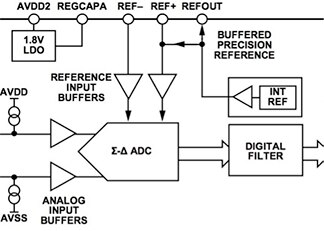
Figure 5: The Analog Devices AD7175-8 sigma-delta ADC combines a buffered internal voltage reference with separate buffers on the reference inputs to the ADC itself. (Source: ADI)
Linear Technology combines an integrated bandgap reference with an on-chip buffer amplifier that designers can select or deselect as needed to suit their unique requirements (Figure 6).
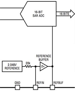
Figure 6: The Linear Technology LTC2345-16 SAR ADC includes an on-chip reference buffer amplifier on the output of its integrated bandgap voltage reference. (Source: Linear Technology)
With the Linear LTC2345-16, designers can take advantage of the internal buffer in using an external reference (Figure 7a) or bypass it entirely (Figure 7b). Because the LTC2345-16's internal buffer is limited to 4.4 V maximum, designers need to bypass the internal buffer when using this ADC with a 5 V reference such as the LT1027-5 (or LTC6655-5 as illustrated in Figure 7b).

Figure 7: With the Linear LTC2345-16 ADC, designers can choose to use (A) or bypass (B) the device's integrated reference buffer when using an external precision voltage reference, shown here with devices from the LTC6655 family. Because the reference buffer maximum voltage is 4.4 V, designers must bypass the on-chip buffer when using a 5 V reference (illustrated in B). (Source: Linear Technology)
As shown in Figures 5 and 6, advanced ADCs such as the Analog AD7175-8 and Linear LTC2345-6 integrate bandgap voltage references on-chip along with associated buffers. Typically, selecting the internal reference is as simple as adding a decoupling capacitor across the appropriate IC pins. For example, designers select the Linear LTC2345-16 ADC's internal reference by simply removing the external voltage reference shown in Figure 7a and replacing the 2.7 μF capacitor shown in that figure with a 0.1 μF capacitor.
Even with these ADCs, the respective manufacturers will note that use of external voltage reference devices will result in better accuracy due to the lower noise figures and temperature coefficients of those ICs. Although noise specifications for on-chip voltage references are not always specified in datasheets, engineers can find data showing the improvement in integral nonlinearity associated with use of an external reference (Figure 8).
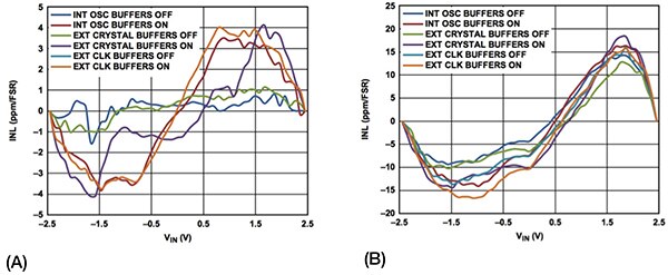
Figure 8: Manufacturers typically do not provide detailed characteristics for voltage references integrated on ADCs, but datasheets may show the impact on performance and accuracy. For example, the data sheet for the Analog Devices AD7175-8 ADC includes charts that describe the device's integral nonlinearity (INL) using an external 2.5 V reference (A) and using the internal 2.5 V reference (B). (Source: Analog Devices Inc.)
Conclusion
IoT sensor applications present designers with a significant challenge in achieving a suitable balance between requirements for measurement performance and those for design simplicity. In addressing these requirements, the choice of voltage reference underlying ADC operation is a critical factor in achieving the ideal balance. Integrated in ADCs, on-chip voltage reference sources and companion buffers provide the simplest design solution. For more demanding IoT sensor applications, however, engineers can combine external voltage reference devices with noise reduction and buffering strategies to optimize measurement accuracy available with advanced high-resolution ADCs.

免责声明:各个作者和/或论坛参与者在本网站发表的观点、看法和意见不代表 DigiKey 的观点、看法和意见,也不代表 DigiKey 官方政策。


