Moving to the Digital Domain for Power Conversion
投稿人:DigiKey 欧洲编辑
2016-09-27
There are many aspects to the generation, distribution and consumption of power, generally involving multiple stages of conversion from one form to another, with each stage exhibiting its only variety of conversion and control. The underlying method of conversion is generally most efficiently achieved through switching the source voltage in a way that can deliver rectification, step-up or step-down conversion or even inversion.
The predominant form of switching is now Pulse-Width Modulation (PWM), which offers a high level of control over the output waveform/voltage and, therefore, can also deliver the greatest levels of efficiency. Implementing a PWM control stage in power conversion can (and has been) achieved in the analog domain, but while this may offer an acceptable solution under specific conditions, it offers little flexibility and can result in solutions that may not be able to provide efficient conversion over a wide range of operating conditions. For this reason, the control of PWM conversion stages is now transitioning to the digital domain and at the heart of this new paradigm is the microcontroller (MCU). It offers the ability to not only add flexibility to a design but drive up efficiency. Of course, this comes at a cost in terms of complexity, so what are manufacturers doing to ease this transition?
Still analog
The good news, for analog designers, is that digital power conversion still involves a significant amount of analog technology; MOSFETs are still used to switch and direct power. The bad news, for those not familiar with MCUs, is that the PWM signals used to control those MOSFETs are now generated by an algorithm.
This could clearly cause some consternation for engineers not familiar with writing embedded code, however many of the leading manufacturers targeting this application space now provide software libraries intended to help designers in the first instance, such as the Switched Mode Power Supply Control Library offered by Microchip; a library that has been optimized for the dsPIC33F and dsPIC33E family of Digital Signal Controllers.
Although very similar to ‘traditional’ MCUs, the devices now known as Digital Signal Controllers (DSCs) are a relatively new class of device developed for just this type of application. For example, the dsPIC33E features a high-speed PWM block that offers up to three PWM pairs each with independent timing, and able to support DC/DC, AC/DC conversion with Power Factor Correction, as well as inverter design, lighting control and BLDC (Brushless DC Motor) control.
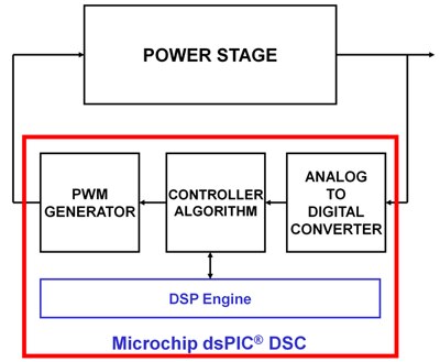
Using a dsPIC in digital power applications effectively means the DSC replaces several functions in an analog-only design; the summing node (which compares the voltage at the converter’s output with a reference voltage), the compensator (the part of the design that implements feedback to ensure stable operation), and the PWM generator itself can all be subsumed by a DSC.
In a digital topology, the algorithm used effectively replaces the compensator hardware. Because it’s software, it offers much more flexibility, such as the ability to implement non-linear functions. This allows much more freedom in system design when it comes to dealing with supply variations or load changes. In addition, modifications are made much more readily, without the need to remove or adjust physical components; instead changes can be made by simply altering a few digital parameters. Figure 1 shows a block diagram of the analog functions that can be replaced by a dsPIC DSC in a digital power design.
One further element required in a digital design that isn’t apparent in a traditional analog solution is the ability to measure the voltage(s). This provides data vital to the digital control algorithm and is achieved through Analog/Digital Converters (ADCs). The dsPIC33E features an ADC module with up to 16 analog inputs that can sample at up to 1.1 Msamples/s. This level of performance significantly increased the functioning frequency of a DSC.

Figure 1: Microchip Technology’s dsPIC33 has been designed to replace several analog functions in a power conversion design.
Comprehensive design support
It is apparent that digital power conversion still relies heavily on analog functionality, which is why MCUs in general and DSCs in particular are well suited to this application space; they combine the digital capability of a processing core with essential analog features — such as ADCs and DACs, operational amplifiers and comparators — in a single device.
The close integration of the two domains is crucial, as it allows control loops to be optimized in the time domain. Minimizing conversion time in the feedback loop can be critical to increasing overall efficiency, which is ultimately the aim of any digital power conversion solution.
This is evident in the XMC4500 family from Infineon, which combines many features designed to make highly efficient digital power conversion simpler to achieve. This includes a high-resolution PWM (HRPWM) that offers a duty cycle resolution of 150 ps. With such fine adjustment possible, the output voltage of a buck converter can be regulated more accurately, resulting in less output voltage ripple, for example.
The HRPWM is supported by the capture/compare units in the XMC4500: CCU4 and CCU8. These units can support a wide range of pulse generation, including asymmetric, aperiodic and single-events. The units can also be triggered by a number of internal/external sources or detected events.
Another benefit of using a programmable device at the heart of a power conversion solution is that it can readily implement the Power Management Bus protocol (PMBus); an open standard that features a command language with over 200 instructions, designed to allow different and disparate elements of a system to communicate. Based on the I2C interface and a variant of the System Management Bus (SMBus), it is relatively simple to add PMBus slaves to a system based on the XMC4500; an application guide is available on the Infineon site that explains how this can be achieved. There is also support for designing power conversion solutions using the XMC4000 family in Version 4 of Infineon’s software development platform, DAVE.
The XMC4000 family is based on the ARM Cortex-M4 core with floating point extensions, a 32-bit core with many advanced features and which is fully integrated with Infineon’s CCU4/CCU8 and HRPWM functions. Infineon offers a range of DAVE apps for power conversion and PWM generation using the HRPWM module. As such, it is a comprehensive platform suitable for even the most complex power conversion systems.
The importance of PWM
While many DSCs are based on a core originally designed for MCUs, some take the approach of using a DSP (Digital Signal Processor)-based core and marrying it with the hardware features needed for a DSC solution. A good example of this type of device is the TMS320F2802x Piccolo MCUs from Texas Instruments. Perhaps more significant than its core, however, is the enhanced PWM peripheral. This is a highly programmable and largely autonomous peripheral that, once configured, is able to run with only the minimum of CPU interaction. This clearly offers advantages in real-time systems such as complex power conversion.
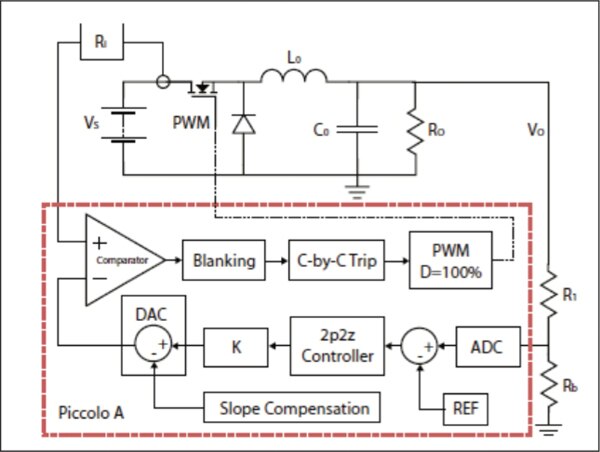
Each ePWM features a 16-bit time-base counter and supports two PWM outputs, which can operate independently. They also feature eight sub-modules including the time-base counter, which is joined by (amongst others) a Dead-band submodule for traditional complementary control of upper- and lower-switches, and a PWM Chopper used to create a chopping carrier frequency if required. A High-Resolution extension to the PWM (HRPWM) is also available on some variants. Figure 2 shows how the Piccolo could be used in a Peak Current Mode Control (PCMC) buck converter.

Figure 2: Texas Instruments’ Piccolo DSC in a peak current mode control buck converter configuration.
The ability to merge an MCU core with DSP-like features to create a DSC is a clear benefit in digital power applications, which is effectively what the 56F8037/56F8027 family from NXP (formerly Freescale Semiconductor) also offers. Based on a dedicated core with a dual Harvard architecture, its single-cycle design means it can execute up to 32 million instructions per second running at just 32 MHz. This is aided by the single-cycle 16 x 16-bit parallel MAC (multiplier-accumulator) unit. While the core frequency is just 32 MHz, the PWM can operate from a clock running at up to 96 MHz with 15-bit resolution. The six-output PWM module allows a source signal to be supplied from either the PWM generator, an external GPIO, an internal timer, an analog comparator output or from an ADC conversion.

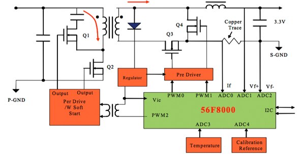
Figure 3: This diagram shows how NXP’s 56F8000 provides digital control in an isolated 110 W DC/DC SMPS.
Figure 3 shows a block diagram of the 56F8000 as it would be used in a DC/DC SMPS application, in this example it is a 110 W isolated switch-mode power supply, with the DSC on the secondary side.
Conclusion
The migration to digital power has been in evidence for some time; the benefits of digital control are hard to deny, and thanks to the continued and aggressive advances made in analog and digital integration on a single device, it is now more cost-effective than ever to adopt a digital power solution.
Demand for more power-efficient operation is only increasing, which is naturally contributing to the move towards digital control. With so many capable solutions now available, it is clear that a move to digital power conversion is not only commercially appealing but also technically rewarding.

免责声明:各个作者和/或论坛参与者在本网站发表的观点、看法和意见不代表 DigiKey 的观点、看法和意见,也不代表 DigiKey 官方政策。


 中国
中国