Low-Noise Amplifiers Maximize Receiver Sensitivity
投稿人:电子产品
2012-06-07
In every RF receiver system, such as those found in base stations, cell phones, GPS units, wireless LAN interfaces, and other applications, low-noise amplifiers (LNAs) can be used to improve the signal-to-noise ratio by replacing amplifiers with higher internal noise levels. The noise signals in these systems come from external sources (extrinsic) and internal circuit component sources (intrinsic), exhibiting a wide range of characteristics for which designers can calculate and compensate. Extrinsic noise sources can be filtered to provide a cleaner signal to the amplifier and, by prudent design and selection of the amplifier, the signal-to-noise ratio (SNR) can be maximized.
Noise figure (NF) is a design parameter that describes the amount of additive noise contributed by an amplifier in the signal chain. Noise can degrade an analog signal or the bit and frame error rates of digital communication systems. In radar systems, receiver noise will limit the effective range of the radar. Ideally, designers should optimize the overall SNR to provide the best system performance possible. Noise figure is defined as the noise factor, F, expressed in decibels [NF = 10 × log (F)], with F defined as (Si/Ni)/ (So/No), the ratio of the SNR at the input to the SNR at the output.
All amplifiers have some amount of thermal noise and other types of noise that they add to the signal they are trying to amplify. And since most RF signals are relatively weak when they reach the receiving antenna, the amplification process should introduce as little noise as possible to deliver the cleanest signal to the rest of the system. In many applications, multiple gain stages are cascaded to greatly improve the signal strength. The Friss equation shows that the noise figure, F1, of the first receiver stage dominates the added noise, and subsequent stages have progressively lower impact on the total noise.
F = F1 + (F2 – 1)/G1 + (F3 – 1)/ (G1×G2) + …, where Gn is the gain of the nth stage in the receive chain.
For example, an NF of less than 1 dB and gain of 30 dB are common requirements, in addition to good linearity. In wireless base stations, receiver amplifiers are often connected to non-ideal sources (e.g., antennas with long cables), and LNAs can help compensate for these non-ideal sources. Typical signal levels expected at the LNA output include the amplified received signal and the antenna (source) thermal noise that was boosted by the LNA, plus the LNA noise figure and any narrowband interfering signals
To deal with the noise, specially designed LNAs offer noise figures of as little as 0.6 dB. Although CMOS technology has propagated through almost the entire system, LNAs are often fabricated using gallium-arsenide, enhancement-mode pseudomorphic high-electron-mobility transistors (GaAs pHEMTs), or bipolar silicon-germanium transistors (SiGe) to keep the noise levels as low as possible. For solutions with NF levels over 1 dB, CMOS has made some inroads, and one vendor, Torex Semiconductor , offers a CMOS LNA, the XC2401A8167R-G, that has an NF of 0.69 dB at 1.575 GHz when powered from a 1.2 V supply. The chip is targeted at GPS receiver applications and has internal self-biasing to eliminate the need for external bias settings. Thus, the LNA’s footprint is very small—just 0.75 x 1 mm—ideal for mobile GPS systems.
When evaluating LNAs, there are three main parameters to look at: the NF, the gain, and the linearity. In the wireless infrastructure, for example, tower-mounted LNAs are routed through long cables to the base station. Thus, higher gain is needed to overcome cable losses. Linearity is also important because the RF spectrum in the vicinity of the tower can be very crowded and higher linearity helps the system separate the signals. LNAs can also be loosely grouped into devices targeted at the portable/battery-powered market with current drains of less than about 10 mA, and devices targeted at system infrastructure, which have operating currents of up to about 100 mA.
For portable systems, Avago Technology, California Eastern Labs (CEL), RFMD, and Skyworks offer GaAs-based LNAs, while Infineon, Maxim Integrated, and offer SiGe-based LNAs. Many of the same products can also be used for infrastructure systems, but some of the same companies also have LNAs that consume a bit more power, typically drawing 30 to 100 mA from a 5 V supply, that deliver wider bandwidths or more gain to better meet the performance requirements of base stations, hotspots, and other infrastructure systems.
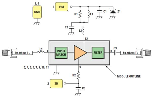
Avago, for example, offers a wide range of LNAs, all based on GaAs pHEMT technology. Some are targeted at GPS systems, such as the ALM-1412 (Figure 1), which operates over a wide voltage range of 1 to 3.6 V, has NF of 0.82 dB at 1.575 GHz, a gain of 13.5 dB, and a standby/off current drain of less than 100 nA (Figure 1). Offering a similar solution in SiGe, the Maxim MAX2659 offers a higher gain of 20.5 dB and a slightly lower NF of 0.8 dB. In its active mode, the chip draws 4.1 mA from a 1.6 to 3.6 V supply; however, in standby the chip current drops to about 1 µA. NXP also has a SiGe solution, the BGU7005 that targets GPS applications with a NF of 0.85 dB, an active current of 4.5 mA, and a standby current of less than 1 µA. Adding carbon to the SiGe process, designers at Infineon developed the BGU7007, an LNA with a 0.85 dB NF and a gain of 18.5 dB. Like the other GPS LNAs, the BGU7007 operates with a supply ranging from 1.5 to 3.6 V, and consumes just 4.8 mA when active and less than 1 µA on standby.

Figure 1: A low-noise solution for GPS systems the ALM1412 from Avago has a NF of 0.82 dB and can be put into a very-low-current standby state, drawing less than 100 nA.
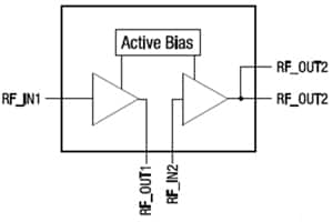
Targeting infrastructure systems, Skyworks offers a wide selection of GaAs LNAs. Two devices in the family, the SKY67014-396LF and SKY67106-306LF, both offer a bandwidth of 1.5 to 3 GHz. However, the first LNA has a NF of 0.9 dB, while the latter offers a low 0.65 dB NF. The SKY67014 is a single-stage LNA with a gain of 12 dB at 2.45 GHz and has both active bias and a stabilization network. The LNA has an operating current of 50 mA from a 5 V supply and fits in a 2 x 2 mm, eight-contact DFN package. In contrast, the SKY67106 consumes about double the current due to its two-stage design employing pHEMT devices on the first stage and heterojunction bipolar transistors (HBTs) on the second stage, all in a 4 x 4 mm surface-mount package (Figure 2). The chip delivers almost three times the gain (35 dB) of the single-stage LNA and includes active bias control to simplify the overall system design.

Figure 2: A two-stage LNA developed by Skyworks combines both GaAs pHEMT transistors for stage one and HBTs for stage two for a total NF of just 0.65 dB and a gain of 35 dB.
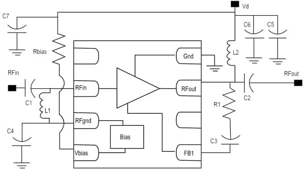
Avago also has some GaAs solutions for infrastructure. The MGA631P8 includes active bias and delivers an externally adjustable gain of 15-20 dB and an extremely low noise figure of just 0.53 dB. The chip also has good linearity, offering an IP3 output of 32.6 dBm. Operating from a 4 V supply, the LNA has an adjustable supply current of from 40 to 80 mA. System designers can adjust the chip’s supply current and gain externally; due to the high isolation between the input and output, the gain can be adjusted independently through a resistor in series with a blocking capacitor from the output pin to the FB1 pin without affecting the noise figure (Figure 3).

Figure 3: The MGA631 LNA from Avago allows designers to independently set the gain and supply current through a series resistor and blocking capacitor connected between the RF output pin and the feedback pin.
Applying SiGe:C for infrastructure LNAs, designers at NXP crafted the BGU7051, which offers a noise figure of just 0.65 dB at 900 MHz. The LNA was designed to deliver a high linearity of 33 dBm (third-order intercept point, IP3o) at 900 MHz, but has an available bandwidth of 0.5 to 1.5 GHz and a typical gain of about 21 dB.
In addition to the judicious selection of the LNA to meet your system requirements, the design of the printed-circuit board is a critical element of the overall system. Proper attention to ground planes, isolation, and power supply filtering are all key aspects to keep in mind to minimize system noise.
免责声明:各个作者和/或论坛参与者在本网站发表的观点、看法和意见不代表 DigiKey 的观点、看法和意见,也不代表 DigiKey 官方政策。


