How to Use Multiband Embedded Antennas to Save Space, Complexity, and Cost in IoT Designs
投稿人:DigiKey 北美编辑
2022-06-29
Antenna design can make or break a wireless product. The challenge is even greater for an increasingly diverse array of wireless Internet of Things (IoT) designs where regulations limit the transmit power in the allocated frequency bands, even as the engineer strives to maximize throughput and range.
Conventional design guidelines advise strip antennas with a length of half the wavelength of the signal it is intended to receive. For a dipole antenna, this translates to 6.25 centimeters (cm) for the 2.4 gigahertz (GHz) frequency band. But for wireless IoT products, this design advice presents two major challenges. First, space is typically at a premium, so accommodating a relatively lengthy antenna is difficult. Second, IoT products typically access multiple radio frequencies to connect to Bluetooth low energy (Bluetooth LE), Wi-Fi, GPS, and/or cellular. This means having to accommodate multiple antennas, each requiring their own impedance matching circuit, which adds to the cost, complexity, and bulk of the design.
Embedded antennas offer a solution to the space and cost constraints of multiband IoT product design. These monolithic antennas feature compact dimensions and can cope with several different frequencies while offering good performance. However, there is a trade-off: in a like-for-like application, the performance of a multiband embedded antenna will fall short of a single-band strip antenna. This makes it even more important that the designer closely adheres to key design guidelines to maximize the embedded antenna’s efficiency across all operational frequencies.
These guidelines extend beyond just antenna selection and positioning; the embedded component forms just one part of the “antenna system.” To construct an efficient system, the antenna must be carefully paired with a suitable printed circuit board (pc board) ground plane and impedance matching circuit to optimize performance. The design of each part of the system significantly affects the overall antenna system efficiency, and the design of the impedance matching circuit can be particularly challenging for multiband embedded antennas.
This article provides a brief introduction to antennas and the challenges facing designers of wireless IoT devices. It then introduces multiband embedded antennas and explains how to design them in and ensure they are matched with the ground plane and impedance matching circuit to optimize performance.
Antenna basics
An antenna converts voltage and current to produce the transmitted RF signal, and in turn, it converts an incoming RF signal to voltage and current at the receiver. Optimizing the antenna’s efficiency ensures it converts as much of the transmitter power into radiated radio energy and harvests as much energy as possible from the incoming signal to feed the receiver. The efficacy with which it performs these roles largely determines the range and throughput of an IoT device.
Antenna efficiency (typically measured in decibels (dB)) is determined by several factors, but a key factor is impedance. Significant mismatch between the antenna’s impedance (which is related to the voltage and current at its input) and the impedance of the voltage source driving the antenna, results in poor antenna efficacy. The key to boosting efficacy is to equalize the two impedances.
Any power reflected by an antenna on a transmission line due to impedance mismatch interferes with the forward traveling power and creates a standing voltage wave. A common measure of how well the impedance is equalized is the voltage standing wave ratio (VSWR). A VSWR of 1 indicates no impedance mismatch loss, while higher numbers indicate increasing losses. For example, a VSWR of 3.0 indicates about 75 percent of the power is delivered to the antenna. A VSWR of 6 or more indicates poor efficiency and the design should be revised (Table 1).
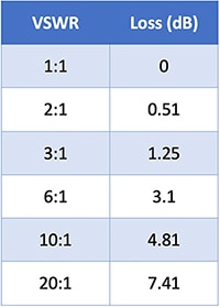 Table 1: High VSWR causes greater losses. The designer should consider revising the design if VSWR exceeds 6:1. (Image source: Steven Keeping)
A further complication is that antenna impedance changes with frequency. This is not a problem when the system is tuned to a single frequency, but IoT products often use radios operating at multiple frequencies. This is necessary to accommodate a mix of multiple interfaces, such as Bluetooth LE (2.4 GHz), Wi-Fi (2.4, 5, and increasingly 6 GHz), LTE-M/NB-IoT cellular (operating on several bands in the 700 to 2200 megahertz (MHz) allocation), and GPS (1227 and 1575 MHz).
One option for multiband products is to use a separate impedance-matched antenna for each frequency, but that adds considerable complexity, size, and expense. An alternative is to use a single embedded antenna and design circuitry to ensure good impedance matching to cover a range of operational frequencies.
Antenna selection and placement
There are several vendors offering mature embedded antenna designs. With knowledge of the end product’s intended operational frequency band(s), it is relatively simple to narrow down the shortlist of suitable antennas from a supplier catalogue. For example, Ignion (formerly Fractus Antennas) offers a range of components suitable for IoT products, including the ALL MXTEND NN02-220 antenna and the TRIO MXTEND NN03-310 antenna.
The NN02-220 is a multiband antenna suitable for cellular 2G, 3G, 4G, and 5G, plus NB-IoT/LTE-M cellular applications and is supplied in a 24 x 12 x 2 millimeter (mm) package. With appropriate system design, the antenna can reach an efficiency approaching 70% and a VSWR of less than 3:1. It features an omnidirectional radiation pattern, providing approximately equal transmission and reception in all directions.
The NN03-310 covers the same frequency bands as the NN02-220 but adds GNSS, Bluetooth LE, Wi-Fi 6E, and ultrawideband (UWB). It measures 30 x 3 x 1 mm and has performance figures similar to its sister product with efficiency approaching 65%, a VSWR of less than 3:1, and an omnidirectional radiation pattern (Figure 1).
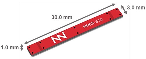 Figure 1: The Ignion NN03-310 is an embedded antenna for cellular, GNSS, short-range RF, Wi-Fi, and UWB. (Image source: Ignion)
Once the embedded antenna has been selected, the next step is to consider the ground plane. The size of the ground plane has a large impact on antenna efficiency. For example, at an operational frequency of 900 MHz, in a like-for-like comparison, a 10 cm2 ground plane might exhibit 30% efficiency, whereas a 40 cm2 ground plane would boost the efficiency to 60%. Therefore, within the constraints of the end-product form factor, it is good design practice to use as large a pc board as possible and then dedicate one complete layer of the pc board to the ground plane. Note that as the frequency increases, the ground plane size has less impact on antenna efficiency. Above a few GHz, the impact is negligible.
The position of the antenna on the pc board also has a large influence on the design’s transmit power and receive sensitivity. Manufacturer guidelines recommend placement at the corner of the IoT device. It is also important to place the chip antenna as far as possible from other active components that could generate electromagnetic interference (EMI) during operation. For the transmission power levels typical of cellular IoT devices, a minimum clearance area of 20 mm from other components is satisfactory. The ground plane should also be kept clear of this area.
The pc board pads and traces connecting the chip antenna to the rest of the circuitry should be the only copper conductors in the clearance area. It’s also good practice to keep the antenna away from housing screws, brackets, and other metallic parts. For example, on the Nordic Semiconductor nRF6943 cellular IoT development board, the antenna is placed at one side of the board with a gap between it and the other components, and at a distance from the mounting screw (Figure 2).
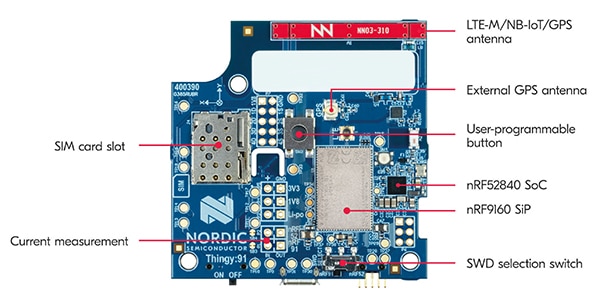 Figure 2: The nRF6943 cellular IoT development board showing the position of the multiband antenna at the top, with wide clearance area (partially covered by white label) between the antenna and other components. (Image source: Nordic Semiconductor)
The nRF6943 is designed to assist engineers in the development of IoT devices using short-range wireless (Bluetooth LE), LTE-M/NB-IoT, and GPS.
Matching circuit design
The most important part of the antenna system design is the impedance matching circuit, which sits between the chip antenna and the IoT device’s transceiver. The purpose of the matching circuit is to limit transmit/receive losses by matching the impedance of the transmitter power sources with that of the antenna (typically 50 Ω for a low-power IoT product).
The engineering task is to not only design the appropriate circuit topology, but also to select the appropriate inductor and capacitor values to “transform” the voltage source impedance such that it matches the antenna impedance. The use of high-quality factor (Q) and tight tolerance components enhances performance. For a single operating frequency band, for example 2.4 GHz, the design is relatively straightforward, but for an IoT product operating in multiple frequency bands, the matching circuit becomes much more complex.
To assist designers, antenna suppliers such as Ignion offer software that makes the job much easier. Armed with knowledge of the pc board size, choice of chip antenna, frequency band requirements, and S11 parameters (the reflection coefficient for the system which is a proxy for the target efficiency), designers can use Ignion’s software package to not only design the matching circuits, but also determine the exact component values needed to approach the S11 parameter target. With the assistance of the software, provided the pc board is large enough, it’s possible to design an antenna system with just one embedded antenna and matching circuit that meets the needs of a full multiband system.
However, if the pc board (and hence the ground plane) is small, a multiband antenna system with a single matching circuit can fail to perform well. One solution—employed on Nordic’s nRF6943—is to incorporate more than one matching network, with each accessed as needed through an MCU-controlled switch. The benefit of doing this is improved performance across all frequency ranges, with the downside that cost and complexity increase when compared to a single matching circuit. These downsides are mitigated to an extent because each matching circuit only needs to transform the impedance for a single frequency band, and will consist of just a few components.
Figure 3 shows an example of the NN03-310 used in a reference design on a small pc board using three matching circuits (or matching networks (MN) as Ignion calls them). MN sections a, b, and c form the matching circuit for operation in the 824 – 960 MHz and 1710 – 1990 MHz cellular bands; MN sections d and e suit the 1561 – 1606 MHz GNSS frequencies; and MN section f is the matching network for 2.4 GHz (Bluetooth LE or Wi-Fi) operation. Figure 4 shows the design and component values for the cellular matching circuit (section a, b, and c), and Figure 5 shows the simulated performance of the complete design.
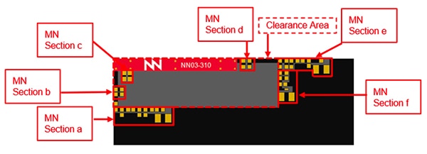 Figure 3: Reference design using the NN03-310 antenna in a multiband design showing the matching circuit positions. (Image source: Ignion)
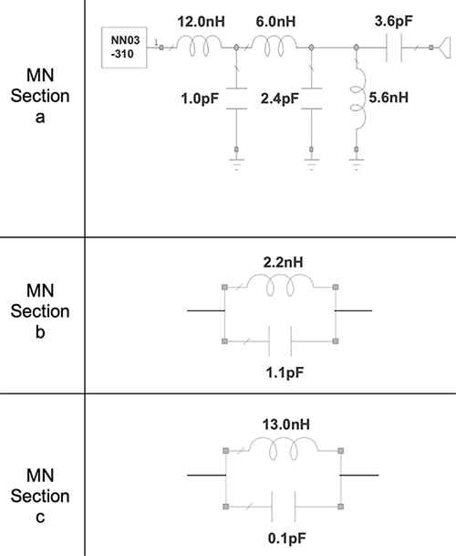 Figure 4: Matching circuit for sections a, b, and c (cellular operation) shown in Figure 3 with component values calculated using the Ignion design software. (Image source: Ignion)
 Figure 5: Simulated VSWR and efficiency results for the reference design shown in Figure 3, using the NN03-310 and matching circuit’s component values calculated by the Ignion design software. (Image source: Ignion)
Testing the antenna system
Even though the matching circuit software will provide a good estimate of antenna system frequency response and efficacy, an actual prototype must be tested to ensure it demonstrates not only the predicted radiative efficiency, but that it is also approximately omnidirectional.
The first test can be done by connecting a 50 Ω micro-coaxial cable to the antenna, grounded at three or four points on the pc board, and then connecting that cable to a network analyzer. The results will not only indicate efficiency but also frequency response and bandwidth. The test typically reveals if some adjustment to the matching circuit components is needed.
Ignion has made initial testing easier by supplying evaluation boards for both the NN02-220 and NN03-310 antennas, the EB_NN02-220-1B-2R-1P and EB_NN03-310-M+5G, respectively. In each case, the evaluation boards include the antenna, impedance matching circuits, and the grounded 50 Ω micro-coaxial cable (Figure 6).
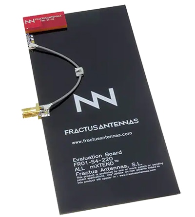 Figure 6: The Ignion antenna evaluation boards include a grounded 50 Ω micro-coaxial cable which can be connected to a network analyzer. (Image source: Ignion)
A designer can plug the evaluation boards into a network analyzer to familiarize themselves with the frequency response they might expect from a similar prototype design, before moving on to product testing.
The final examination of the cellular IoT device’s performance should be made in an anechoic chamber. This is the ultimate test of a design which often reveals weaknesses in efficiency and omnidirectional performance that don’t show up during network analyzer testing. Deficiencies might require a revised embedded antenna selection, ground plane and clearance area redesign, and/or matching circuit tuning.
Conclusion
The small size and multi-frequency operation of many IoT products makes antenna implementation a challenge. Separate antennas and matching circuits for each frequency can be tough to accommodate, and they add complexity and cost.
Embedded antennas offer an option to save space by using a single device to serve multiple frequencies. The trade-off is that ground plane, clearance, and matching circuit design becomes even more difficult. However, embedded antenna suppliers offer proven design advice and software modeling tools that can ease the design cycle. Even with this assistance, the task is not trivial, and antenna system design often comes down to repeatedly testing a design’s performance and then refining the layout.

免责声明:各个作者和/或论坛参与者在本网站发表的观点、看法和意见不代表 DigiKey 的观点、看法和意见,也不代表 DigiKey 官方政策。


