Generating Isolated Outputs Using Fly-Buck Converter Topology
投稿人:电子产品
2015-09-01
Many applications require simple, inexpensive isolated power supplies as bias, generated from input voltages as high as 100 V. Traditionally, such isolated bias supplies are generated using multiple schemes. One of them is the flyback DC/DC converter, which typically utilizes an asymmetric transformer with turns ratio for primary and secondary windings and an opto-coupler or an auxiliary winding for feedback regulation. In reality, such flyback converters must also incorporate complex compensation techniques for stability. As a result, traditional flyback converters are not simple, require more components and space, and could cost more.
An alternative approach is an isolated-buck or fly-buck DC/DC converter, a synchronous buck converter with coupled inductor windings. According to Texas Instruments’ application report1 “Designing an Isolated Buck (Fly-buck) Converter”, fly-buck is a better option for low-power isolated outputs, especially when the power level is below 15 W. In fact, TI’s application report suggests that its Fly-buck is a cost-effective solution for generating multi-output bias supplies below 15 W. Because Fly-buck uses a synchronous buck converter with coupled inductor windings to create isolated outputs, its transformer is smaller and better matched in terms of primary and secondary turns ratio. Also, as the secondary output closely tracks the primary output voltage, the Fly-buck eliminates an opto-coupler or auxiliary winding1.
Fly-buck topology
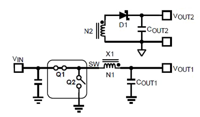
Fundamentally, as shown in Figure 1, a fly-buck topology is created by replacing the output filter inductor in a synchronous buck converter with a coupled inductor or flyback-type transformer X1. The voltage on the secondary winding of this transformer is rectified using a diode D1 and capacitor COUT2. As discussed in Reference 1, the Fly-buck topology can be extended to generate multiple isolated secondary outputs.

Figure 1: A typical fly-buck converter topology. (Courtesy of Texas Instruments)
In essence, the primary output voltage VOUT1 of a fly-buck is similar to a buck converter as depicted below1:
![]()
Similarly, the secondary output voltage VOUT2 is given as:
![]()
Where VF is the forward-voltage drop of the secondary rectifier diode, and N1 and N2 are the number of turns in the primary and secondary windings of the transformer X1, respectively. As shown in equation (2), the secondary output (VOUT2) closely tracks the primary output voltage (VOUT1) without the need for additional transformer winding or an opto-coupler for the feedback across the isolation boundary.
Also, as described in Reference 1, TON is the time when high-side switch Q1 is on and low-side switch Q2 is off. Similarly, TOFF is the time when the low-side switch Q2 is on and Q1 is off. During TON, the current in the secondary winding is zero as the secondary diode is reverse-biased by a voltage equal to VIN x N2/N1. The current in the primary winding is the same as the magnetizing current, which is similar to a buck converter inductor. Calculations for the currents in the two windings are presented in detail in Reference 1.
Implementing topology
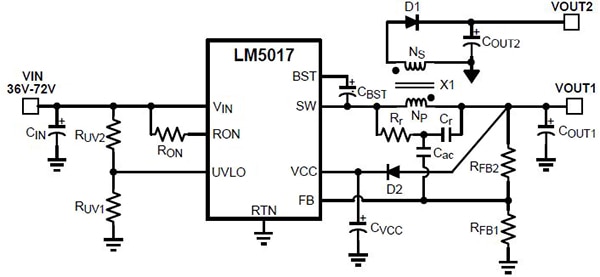
Now the topology shown in Figure 1 can be easily implemented using a conventional synchronous buck regulator like TI’s LM5017, which includes high- and low-side MOSFETs in compact packages like WSON-8 and PowerPAD-8. Since LM5017 incorporates constant on-time control scheme, it requires no loop compensation and provides excellent transient response with the ability to handle high step-down ratios. This buck regulator is rated for a wide input range of 7.5 V to 100 V.
A typical isolated Fly-buck DC/DC converter using LM5017 is shown in Figure 2. It is a two-output circuit with 10 V as the primary-output voltage VOUT1 as well as the secondary-output voltage VOUT2. In this design, the primary load current is 100 mA while the secondary-load current is 200 mA. The switching frequency is 750 kHz.

Figure 2: A typical isolated Fly-buck DC/DC converter based on TI’s 100 V synchronous buck regulator LM5017.
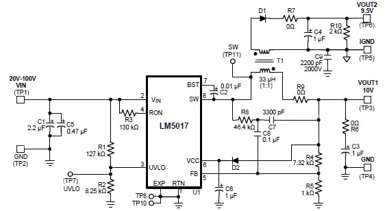
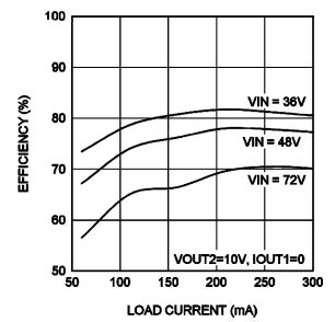
Component calculations for this two-output isolated Fly-buck DC/DC converter are given in Reference 1. Based on the above specifications, the reference provides component values for the LM5017-based Fly-buck converter. These values are implemented in the LM5017-based isolated Fly-buck DC/DC converter schematic, which are illustrated in Figure 3. The reference also provides measured experimental efficiency results for the Fly-buck circuit in Figure 3, which are plotted in Figure 4.

Figure 3: Complete schematic with component values for an LM5017-based isolated Fly-buck DC/DC converter.

Figure 4: Experimental efficiency performance of an LM5017-based isolated Fly-buck with 10 V output and 750 kHz switching frequency.
It is observed that the efficiency of the Fly-buck converter is high when the input voltage is low, which amounts to a smaller step-down ratio. As the input voltage increases, the efficiency begins to drop significantly because the step-down ratio increases which results in higher conversion losses. By comparison, low-load to full-load variation in efficiency also increases as the input voltage rises. As a result, the drop in efficiency at low load is sharper when the input voltage is as high as 72 V.
For applications that require a slightly lower input voltage with higher output current capability, TI offers LM5160A, a synchronous buck converter with 4.5 to 65 V input voltage range and 1.5 A maximum load current. With integrated high- and low-side MOSFETs, and a built-in constant-on-time control scheme, LM5160A requires no loop compensation and supports high step-down ratios with fast-transient response.
In short, for a low-power, multi-output isolated step-down DC/DC-converter solution from a widely varying input voltage, the fly-buck converter is a better choice when very tight regulation is not important for the regulated output voltage, but simplicity, cost, and board space are critical for the application.
For more information on the products discussed in this article, use the links provided to access product pages on the DigiKey website.
Reference
- Application Report AN-2292 “Designing an Isolated Buck (Fly-buck) Converter”, Texas Instruments, May 2013.
免责声明:各个作者和/或论坛参与者在本网站发表的观点、看法和意见不代表 DigiKey 的观点、看法和意见,也不代表 DigiKey 官方政策。


 中国
中国