FRAM ICs Extend Endurance in Low-Power Applications
投稿人:电子产品
2015-04-22
Although EEPROM and Flash have typically been the top choice for non-volatile memory (NVM) in most applications, ferroelectric RAM (FRAM) offers distinct advantages for many low-power designs in energy-harvesting applications such as wireless sensor nodes, smart meters, and other data-logging designs. With its extended write-cycle endurance and data-retention time, FRAM technology can help designers meet requirements for decade-long, low-power NVM operation using available FRAM ICs and FRAM-based MCUs from manufacturers including Cypress Semiconductor, Fujitsu Semiconductor, ROHM Semiconductor, and Texas Instruments.
Conventional NVMs, such as Flash and EEPROM, store data in the form of charge carriers in a floating gate that requires a charge pump to boost voltages to the levels needed to force carriers through the gate oxide. As a result, along with the long-write delays and high-power consumption inherent in these devices, their high-voltage write operation can eventually wear out the cell – sometimes in as few as 10,000 write cycles.
FRAM advantages
In contrast, Ferroelectric RAM (FRAM) stores data by means of the polarization of the ferroelectric material lead zirconate titanate, or PZT (Pb (ZrTi)O3), which is placed as a film between two electrodes similar to the structure of a capacitor. As with a DRAM, each bit in a FRAM array is read and written individually, but while DRAM uses a transistor and capacitor to store the bit, FRAM uses a dipole shift in the crystalline structure for the corresponding bit caused by application of an electric field across the electrodes (Figure 1). Because this polarization remains after the electric field is removed, the FRAM data persists indefinitely even without available power – a vital capability for designs powered by uncertain ambient sources.
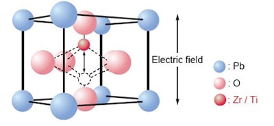
Figure 1: In an FRAM cell, data is stored as the state of polarization caused by application of an electric field across the PZT film – an approach that enables extended data retention and eliminates the wear encountered in floating-gate technologies. (Courtesy of Fujitsu Semiconductor)
Along with enabling FRAM’s non-volatility, the use of crystal polarization offers a number of advantages over technologies based on charge storage (see Table 1). Because it avoids the potential degradation effects of floating-gate technologies, the lifetime of FRAM memory and its ability to retain data in the face of power loss is virtually unlimited. For example, FRAM memory devices such as the Fujitsu Semiconductor MB85R1001A and ROHM Semiconductor MR48V256A all specify 10-year data-retention performance.
| FRAM | EEPROM | FLASH | SRAM | |
| Memory Type | Non-volatile | Non-volatile | Non-volatile | Volatile |
| Write Method | Overwrite | Erase + Write | Erase + Write | Overwrite |
| Write Cycle Time | 150 ns | 5 ms | 10 μs | 55 ns |
| Read/Write Cycles | 1013 | 106 | 105 | Unlimited |
| Booster Circuit | No | Yes | Yes | No |
| Data Backup Battery | No | No | No | Yes |
Table 1: Comparison of FRAM with other memory technologies. (Courtesy of Fujitsu Semiconductor)
By eliminating the need for a charge pump required in floating-gate memory technologies, FRAM can operate at typical supply ranges of 3.3 V or lower. Furthermore, unlike stored-charge memory devices, FRAM devices are resistant to alpha particles and typically exhibit Soft Error Rates (SER) below detectable limits.
Design impact
The impact of FRAM’s advantages ripples through the design of systems, such as wireless sensor nodes, that require a combination of high-speed writes and low-power operation. For example, with its high rate, designers can use a single FRAM device where they might have needed multiple EEPROM devices arranged in parallel to achieve acceptable data-write throughput rates. In those EEPROM designs, while one EEPROM device is completing its write cycle, the controller would initiate a write operation on the next EEPROM device in sequence, and so on. With FRAM, however, all writes occur at the bus speed on a random-access basis, with no memory-based latency or other write slowdown. As a result, FRAM memory typically achieves significantly faster writes than Flash at substantially lower energy requirements.
Designers can also eliminate the need for power-backup strategies required to ensure data integrity. With an EEPROM system, the memory controller must complete a full write cycle to the desired data block size when a power fault is detected – requiring additional energy storage to ensure write-cycle completion in EEPROM-based designs. With its fast cycle times, FRAM is able to complete the writing process even at a sudden power outage, thus ensuring data integrity without the need for complex power-backup methods.
At the application level, FRAM’s fast writing speed and low-power operation also enable continuous measurement in energy-harvesting applications, such as wireless sensors or energy meters. At a given power budget, FRAM devices will be able to complete more read/write cycles at a finer granularity than possible with other NVM technologies.
FRAM also presents developers with a unified memory architecture, enabling flexible partitioning of code and data and permitting a simpler, smaller single-chip memory solution. At the same time, designers can easily protect code stored in FRAM from inadvertent writes using a simple write-protect circuit to provide a programmable block-write protection feature for FRAM-based designs (Figure 2, HC151 multiplexer).
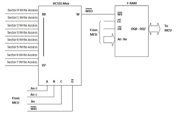
Figure 2: Designers can employ low-power multiplexers such as the HC151 to implement a simple address-dependent write enable capability to protect code stored in the FRAM device. (Courtesy of Cypress Semiconductor)
Device configurations
Designers can find FRAM memories supporting parallel, SPI serial, or I2C/2-wire serial interfaces. For example, along with its parallel 1Mb MB85R1001A FRAM, Fujitsu offers a 1Mb SPI Serial device, the MB85RS1MT, enabling designers to employ an arbitrary number of devices in typical SPI master/slave configurations (Figure 3). Besides operating at lower supply voltages than their parallel counterparts, serial FRAM devices also offer smaller package options for space-constrained designs. For example, the ROHM Semiconductor 32K SPI Serial MR45V032A is available in an 8-pin plastic small outline package (SOP) measuring only 0.154" and 3.90 mm width.
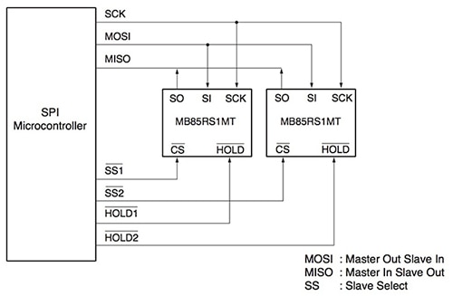
Figure 3: Devices such as the Fujitsu MB85RS1MT allow use of familiar master/slave configurations for SPI-equipped MCUs – or use of simple bus-connectivity solutions using the device’s SI and SO ports for non-SPI-based designs. (Courtesy of Fujitsu Semiconductor)
FRAM technology’s advantages extend to MCUs such as Texas Instruments MSP430FR MCU family with on-chip FRAM. In MCUs, FRAM’s high-speed operation speeds overall processing, allowing write to non-volatile memory to proceed at full speed rather than forcing the MCU into wait states or blocked interrupts. TI’s FRAM MCU family extends from devices such as the MSP430FR5739 to its full-featured MSP430FR5969 series. The smallest device in the MSP430 family, the MSP430FR5739 is available in a 24-pin 2 x 2 die-size ball-grid array (DSBGA), yet includes five timers, a 12-channel 10-bit ADC, and direct-memory access (DMA) for minimizing time in active mode.
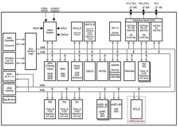
TI’s MSP430FR5969 is the company’s lowest-power MCU featuring a substantial on-chip FRAM store (Figure 4). In active mode, the MCU requires only 100 µA/MHz active-mode current and 450 nA standby-mode current with the real-time clock (RTC) enabled. Devices in this series include a comprehensive set of peripherals and a 16-channel 12-bit analog-to-digital converter (ADC) capable of single- or differential-input operation. These MCUs also feature a 256-bit Advanced Encryption Standard (AES) accelerator and Intellectual Property (IP) Encapsulation module for protecting critical data.
Figure 4: The Texas Instruments MSP430FR5969 MCU combines a full complement of peripherals with on-chip FRAM storage, while requiring only 100 µA/MHz active-mode current and significantly less with its multiple low-power modes (LPM). (Courtesy of Texas Instruments)
Conclusion
FRAM devices offer non-volatile storage with 10-year data retention time at a fraction of the power required with familiar Flash and EEPROM alternatives. Using available FRAM-based memory and MCU devices, engineers can build these robust devices into low-power energy-harvesting applications with confidence in their ability to operate for years and maintain long-term data despite intermittent power loss.
For more information about the parts discussed in this article, use the links provided to access product information pages on the DigiKey website.
免责声明:各个作者和/或论坛参与者在本网站发表的观点、看法和意见不代表 DigiKey 的观点、看法和意见,也不代表 DigiKey 官方政策。







 中国
中国