Developing Anti-Tamper Protection for Wireless Hardware
投稿人:DigiKey 欧洲编辑
2015-05-21
From smartcards to smart meters, there are many different ways a wireless node can be attacked in the Internet of Things. This article looks at the ways devices are protected against all kinds of tampering, from malware code to physical differential power analysis (DPA) and the ways designers can protect against them, including design techniques and implementing physically unclonable functions (PUF).
Protecting the security of information is one of the key challenges in the roll out of the Internet of Things (IoT). Wireless communications are a key technology in this roll out, enabling sensor and control nodes that are easy to install and manage over the Internet. While securing the wireless link through encryption is a key design technique, the wireless node itself can be vulnerable to tampering. This can be to intercept the data being collected, the encryption keys or the code itself. That hacking may be for personal gain, to alter the data in a wirelessly connected smart meter, or international gangs that intercept the data from near field communication (NFC) credit and debit cards.
There are various techniques for tampering, especially for capturing the encryption keys. Once a hacker has access to these, all the data in the system is potentially available, giving all sorts of insights into the activity of the node and as a result into the activity of the wallet, home or factory.
Anti-tampering is a key element in the design of smart meters, NFC chips and wireless IoT nodes, so understanding the attack mechanisms is vital.
The smartcard industry typically places attacks into one of three categories. Non-invasive side channel attacks use information out of the power profile or the electromagnetic emanation, while fault attacks use laser light or glitches in the voltage to change how a chip responds. The power of this technique can be seen in the recent glitch in the Raspberry Pi 2 low-cost computer board that resets when exposed to a camera flash. A third technique is reverse engineering by stripping down the layers of the chip to discover the transistor structure and access data, particularly in the read-only memory, as a result.
The challenge for NFC-enabled wireless smartcards, such as the PN5120 from NXP, is developing sophisticated countermeasures to withstand these new attacks. In some markets, such as electronic passports, smartcard ICs have to withstand attacks in the field for ten years to be valid.
One of these side channel attacks is differential power analysis (DPA). This technique monitors the tiny amounts of energy dissipated in signal lines to determine the bits being transmitted, which has been used to determine the encryption keys that are used in the system. Another of these side channel attacks is to monitor the leakage current that can also lead to the data, while the electromagnetic emission can also potentially provide information about the data being sent.
Countermeasures
DPA countermeasures consist of a broad range of software, hardware, and protocol techniques that protect tamper-resistant devices from side-channel attacks. These include reducing the information leaked into the side-channel to decrease signal-to-noise (S/N) ratios. Designers can also add amplitude or temporal noise into the side-channel to decrease that S/N ratio.
Other techniques include adding randomness into the code to reduce the correlation between side-channels and the original data flow.
Another way to protect against such attacks is to implement a physical unclonable function (PUF). This uses structures within a silicon device to generate a unique number that can also be used to protect against tampering. This is increasingly being used as a way to protect against reverse engineering, as there is no visible data to store that is vulnerable to tampering.
The PUFs are defined as functions based on physical characteristics which are unique for each chip, difficult to predict, easy to evaluate and reliable. These functions should also be individual and practically impossible to duplicate. This means that the PUFs can serve as a root of trust and can provide a key that cannot be easily reverse engineered.
With this technique, the chip itself can check whether the environment is intact. During production or personalization, the IC measures its PUF environment and stores this unique measurement. From then on, the IC can repeat the measurement, usually during start up, and check if the environment has changed, which would indicate an alteration in the card body. This protects against many kinds of invasive attacks.
In principle, any physical device characteristic that fluctuates can be turned into a PUF. One of these is in the SRAM. After powering the Smart Card chip and the internal SRAM, the cells are initialized with a pattern randomly made of zero and one logical values. This pattern is different for each individual chip and small deviations in processing inside the SRAM cell lead to a variation of the electrical characteristics for each transistor. This leads to a small asymmetry resulting in a preferred state (0 or 1) during start up and this serves as a unique fingerprint for the chip and the smartcard.
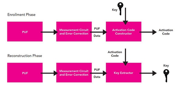
This unique fingerprint is derived using Reed Solomon error correction on the initialization data and this is then used as a key to protect a cryptographic key or to protect a memory location by acting as an internal key. This protects the key from both reverse engineering and DPA attacks as it is always protected. It does this as the key is essentially split into two parts – the SRAM PUF fingerprint and an activation code. An attacker must know both values to reconstruct the key that protects the wireless link.
Using a PUF is typically divided into two phases, Enrollment and Reconstruction (as in Figure 1). The Enrollment Phase occurs just once, when a new key is generated or being stored. The key is put into an Activation Code Constructor, which produces the activation code to be stored in non-volatile memory. In the Reconstruction Phase, the activation code is used in the Key Extractor to reconstruct the key but the actual key is not stored in NV memory. This means the key cannot be derived with the activation code alone; the code and the PUF data must both be available to reconstruct the key.

Figure 1: Enrollment and Reconstruction in a smartcard using a physically unclonable function (PUF).
This implementation also has to be carefully designed and security tested such that the PUF itself is not opening other security attack paths, such as some weaknesses with respect to side channel or fault attacks.

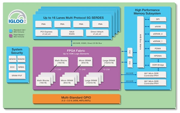
Figure 2: The PUF is a key element in the security of an IGLOO2 FPGA for securing a wireless link in the Internet of Things.
Microsemi has implemented the PUF functionality into its field programmable devices, such as the low power IGLOO2, to add this capability to IoT wireless nodes that are often battery powered. This is being used to demonstrate a Public Key Infrastructure (PKI) for secure machine-to-machine (M2M) communications between embedded systems and for M2M authentication to allow devices to be easily but securely added to an IoT network. Using a non-volatile FPGA, such as the IGLOO2, removes the vulnerability of an external EEPROM and potentially gives a higher level of security. An external device means the bitstream can potentially be intercepted or analyzed to provide information to an attacker, or the EEPROM itself can be reverse engineered.
The approach adopted by Microsemi adds hardened PUF technology that uses dedicated on-chip SRAM and additional countermeasures such as an anti-tamper mesh and dedicated PUF power control. This provides a higher level of security to resist tampering, as the PUF key effectively disappears from the chip when the power is switched off. This means there is no known technology that can read the PUF’s secret while its power is off.

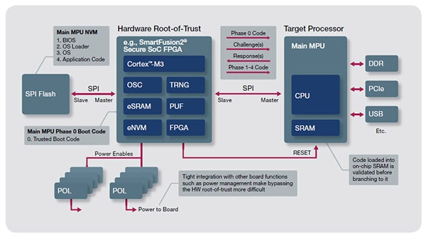
Figure 3: The PUF approach can also be used to implement a secure boot of a microcontroller to prevent tampering.
This approach can also be used to provide a secure boot of the microcontroller in the node, as in Figure 3, to also protect the system from tampering.
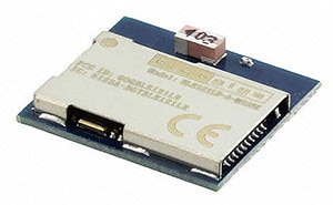
These devices can be used alongside wireless modules such as the BLE121 from Silicon Labs (Figure 4) using protocols like Bluetooth Low Energy to provide the additional security that will prevent tampering. This approach also allows the system designer to keep control of the security aspects of the node and integrate it with the power management while being able to use different wireless modules. This protects both the system IP and the user data at the same time.

Figure 4: Adding an FPGA into a IoT wireless node can help protect a wireless module such as Silicon Lab’s BLE121 from tampering.
Conclusion
Anti-tampering is a key consideration of elements throughout the Internet of Things. From the wireless sensor nodes to the wirelessly connected gateways, from the NFC smartcard to the wireless smart meter, all the systems need to be secured. Using techniques to minimize DPA attacks combined with IP to generate PUF keys can dramatically increase the security of a wireless system.

免责声明:各个作者和/或论坛参与者在本网站发表的观点、看法和意见不代表 DigiKey 的观点、看法和意见,也不代表 DigiKey 官方政策。


 中国
中国