The Flyback Converter
2024-04-15 | By Tobias Bruckmann
Flyback converters are a type of electrical power converter topology for DC/DC conversion. Due to the galvanic isolation between input and output voltage, these converters are used in switch mode power supplies and for high voltage applications like ignition spark converters, but also in other power electronics as auxiliary power supplies. In power electronics applications, they are especially useful for supplying gate driver circuits with power. Below, a simplistic schematic of a flyback converter is shown for us to examine the underlying working principles at play.
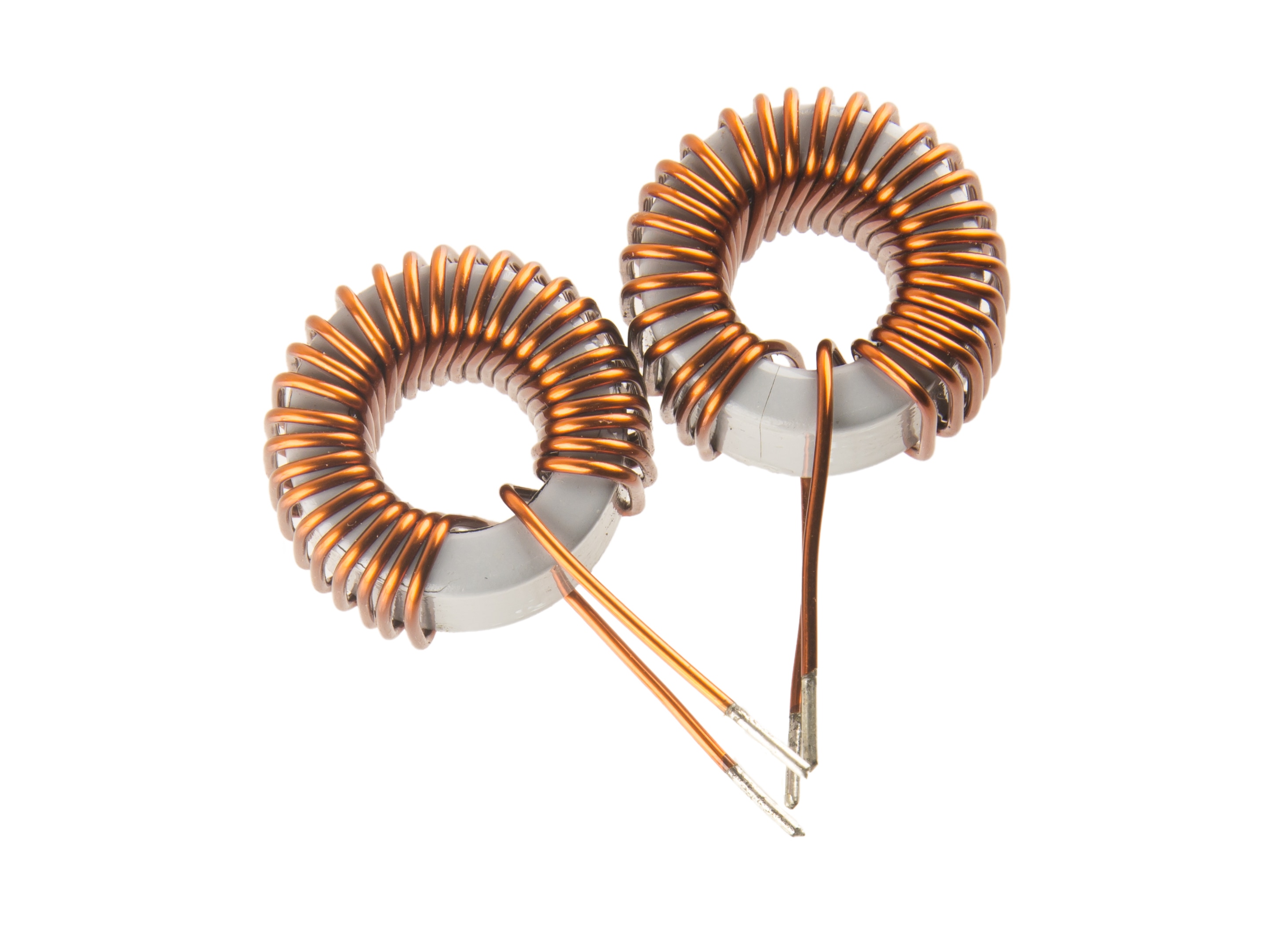
The heart of this circuit is the coupled inductor T1, which in contrast to a transformer employs a gapped core to temporarily store and release energy rather than directly transmitting it from primary to secondary.
Modeling
To get the ideal working principle of the flyback, the following two equivalent circuit diagrams will be examined. The first one is valid for all time intervals in which Q1 conducts.
This second applies when Q1 blocks current.
Q1 conducting Interval
In the conduction Interval of the transistor Q1, V1 is applied over the primary side of T1. Using the differential equation for the I-V characteristic of an inductor.

Approximating Q1 with an ideal switch yields the first equivalent circuit with a linear current increase for the time intervals in which Q1 is conducting. Magnetic field energy is stored inside the coupled inductor during this phase by increasing the magnetic flux through the coupling core. This increase in flux also causes an induced voltage in the secondary winding of T1. But due to the twist in polarity between primary and secondary winding, this voltage is induced with a polarity leading D1 to block it, which justifies the neglect of T1´s secondary and D1 in the equivalent circuit. Any load connected to the flyback's output is therefore powered by the Energy stored in C1.
Q1 blocking Interval
Turning Q1 off would ideally block any current in the primary winding of T1. In reality, there are a variety of effects and imperfections leading to differing behavior and undesirable characteristics during Q1´s turn-off. Staying for now with ideal assumptions, the current through T1´s primary vanishes, justifying leaving out T1´s primary in this equivalent circuit. Due to the coupling nature of T1, the stored magnetic energy can now be used in the secondary of T1. While the voltage over the inductor in Q1´s conducting phase was given by the source V1, it is now given as the negative of the summation of D1´s forward voltage and C1´s voltage due to the polarity flip of the windings. Again, the I-V Characteristic of an inductor describes the resulting behavior, and we get a negative slope in current. This current which commuted from T1´s primary now charges the output capacitor and supplies the load connected to the converter.
Power calculations
As can be seen from the discussions above, the flyback fundamentally scoops energy packets from its input to the output by temporarily storing it as magnetic field energy. Given a fixed input voltage, these energy packets can be calculated in dependence to the on-time of Q1.

Additionally, taking the frequency or off-time into account, the power delivered by the converter can be calculated.

For low diode forward voltages with respect to the output voltage and high coupling factors for the coupled inductor, this equation can be used as a reasonable approximation for the flyback's output power.
The equations above can be derived by integrating the power delivered to T1´s primary during Q1´s conduction phase and are only valid for discontinuous conduction mode.
Have questions or comments? Continue the conversation on TechForum, DigiKey's online community and technical resource.


