Buck Converter Transient Response
2024-04-01 | By Jack Hannum
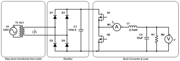
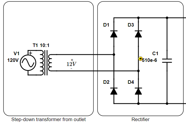
In the last article, we picked out the passives for our buck converter. Soon, we'll design the feedback controls that keep our output voltage regulated nicely regardless of changes in the load or the input voltage. As a reminder, here’s the circuit we’re building, a synchronous buck converter implemented using a MOSFET half-bridge, fed from an outlet through an isolating step-down transformer rectified with a full wave diode bridge.

Why bother with controls?
In steady state, the buck converter produces an output voltage directly proportional to the input voltage: Vout = DVin. We know we have a minimum input voltage of 13.9V, and that we want an output voltage of 3.3V for our microcontroller. That would require a duty cycle of D = 0.237. Why not just give the converter a constant 23.7% duty cycle and be done with it then?
Before even considering transients, we must acknowledge that the input voltage to this converter varies, as it is connected to the grid through an uncontrolled diode bridge rectifier. As developed in Introducing the Rectifier, the output voltage of the rectifier varies between 13.9V and 16.9V over the course of a half-sine wave. If we leave the duty cycle at a constant 23.7%, our output voltage will vary between 3.3V and 4V. Our FRDM-KL25Z microcontroller, which we're powering through its 3.3V pin, can only tolerate a maximum of 3.6V. If we give our converter a constant 23.7% duty cycle with our rectifier's output specs, we'd smoke our microcontroller. We can set the duty cycle to 19.5% so the maximum input voltage gives us 3.3V, but then our minimum output voltage is 2.71V. The microcontroller would work with this output voltage in steady state, but there are still transients to deal with.
In steady-state, buck converters can be modeled as ideal DC transformers, but this relationship breaks down transients, the state between an initial steady state and a final steady state after some change in system parameters, like load current or input voltage. As the rectifier's output voltage changes with a frequency of 120Hz, it never reaches a steady state, constant output voltage. Therefore, we need to consider how the buck converter's output voltage responds to transient changes in the input voltage. Since a lot of a buck converter is an LC filter, the components of which change their impedance with frequency, we should consider how the buck converter output voltage responds to input variations over a range of frequencies.
To get many useful converter transfer functions, we can draw a small-signal equivalent circuit model, which uses basic circuit elements to describe how a converter's responses to input voltage and load disturbances, as well as control variations, change with frequency. These models are developed fully in Fundamentals of Power Electronics, so I'll only refer to the final small signal model of the open loop buck converter, shown below:

Response of the Converter to Input Voltage Variations:
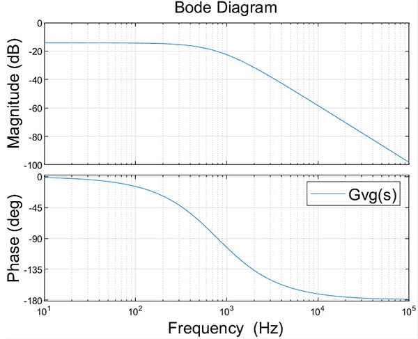
We can do this by drawing the "audio susceptibility" bode plot, which plots an s-domain transfer function Gvg(s) = vout(s)/vin(s) [1]. The transfer function gives us what we're looking for, a relationship between input voltage disturbances and output voltage disturbances.
We can get Gvg from the small signal model above by setting d(t) = 0 and referring vg(t) to the secondary of the transformer. We can write Gvg(s) analytically as

Where the DC gain, Gg0, the resonant peak/trough Q, and the cutoff frequency ω0 vary with converter topology. For the buck converter, the DC gain Gg0 = D, the resonant peak/trough Q = R√(C/L), and the cutoff frequency ω0 = 1/√(LC). For our buck converter, where L = 2.7mH and C = 15uF, and the steady state duty cycle is D = 0.195, ensuring that even in the absence of controls, the microcontroller will not experience a steady-state overvoltage.
Evaluating the above expressions with our circuit's parameters, the DC gain Gg0 is 0.195, or -14.2dB, the resonant Q is 0.498, or -6.05 dB, and the cutoff frequency is 4983 rad/s. These features can be observed in the bode plot below.

At 120Hz it can be seen in the plot that Gvg(s) = vout(s)/vin(s) is -14.4dB, or 0.1905V of change in output voltage resulting from a 1V change in the input voltage. Thus our 3V ripple in input voltage over the course of a pulse will cause a 0.57V ripple in the output voltage seen by the microcontroller; our max voltage will remain 3.3V, but our minimum voltage will be 2.73V. Note that since the gain at 120Hz (0.1905) is nearly identical to the DC gain (0.1945), the minimum output voltage calculated by reading the bode plot is close to that calculated using the steady-state DC relationship, 2.71V. One of the goals of our control scheme will be to reduce the gain of Gvg at 120Hz, such that a smaller change in voltage will occur in response to a 1V change in input voltage.
Response of the Converter to Load Variations:
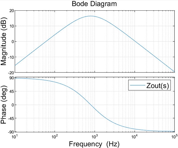
Another reason we want to include controls in our design is the fact that the load may change. Thus far we've designed our converter to run at a constant 0.5A load. But what if the microcontroller draws more or less than that? We need the output impedance of the converter, a transfer function Zout(s) = -vout(s)/iout(s), which relates a change in load current to the resulting change in output voltage. The negative sign just means that an increase in load current coming out of the converter causes a decrease in voltage rather than an increase; this makes sense when you consider that positive load current discharges the output capacitor.
We can get the output impedance of the buck converter by setting vg(t) and d(t) to zero. The current sources become open circuits, and the voltage sources become shorts; the short can then be pushed through the transformer resulting in a parallel RLC network. We can construct the output impedance Zout(s) = sL || (sC)^-1 || R, and plot it as a function of frequency, as below:

This plot shows that even relatively large low-frequency increases in load current will not substantially affect the voltage supplied to the load- at 10Hz, the output impedance is -15.3dB. This means that a 1A increase in load would cause the load voltage to drop by 0.17V. Another goal of the feedback control scheme to be implemented is to reduce this even further.
In the next article, we'll design the feedback controller for the buck converter. With the feedback controls designed, the sensitivity function of the converter will be defined, which will determine the response of many different aspects of the system. Notably, it will reduce the converter's audio susceptibility and output impedance and improve the converter's performance.
[1] R. W. Erickson and D. Maksimović, Fundamentals of Power Electronics. Springer Nature, 2020. doi: 10.1007/978-3-030-43881-4.
Have questions or comments? Continue the conversation on TechForum, DigiKey's online community and technical resource.


