Working with Acceptable Power Levels in Energy Harvesting Applications
投稿人:电子产品
2013-06-26
Ambient energy sources can represent an uncertain power supply in designs using energy harvesting. In these designs, the use of a “power good” signal is particularly important for enabling operation of critical ICs such as MCUs and memory only when power is available at acceptable levels. Engineers can address this issue by drawing on a variety of available solutions from semiconductor manufacturers including Analog Devices, Fairchild Semiconductor, Linear Technology, Micrel, and Texas Instruments, among others.
For energy harvesting designs, the need to rely on trickles of power from ambient energy sources drives a corresponding need not only for careful attention to individual device power consumption and overall power budget, but also the ability to detect when power reaches minimum levels required for circuit operation. For many energy harvesting applications, proper circuit operation entails only recognition that system power has reached the required level. For associated ICs, this recognition comes in the form of a “power good” signal that remains enabled when voltage levels have reached a threshold value set by the engineer.
For more complex designs, engineers can take advantage of sophisticated power management capabilities in dedicated PMICs or specialized energy harvesting devices. For designs intended to minimize device count and system complexity, however, engineers will also discover this functionality built into components typically found at the heart of energy harvesting designs.
Low-dropout (LDO) regulators such as the Texas Instruments TPS797xx family, Fairchild Semiconductor FAN2558, Micrel MIC5248 and MIC5258, and Analog Devices ADP2140, among others, provide a specific “power good” output signal as an open-drain output. Typically used in MCU-based low-power applications, the power good signal provided with this class of device can often be used directly or with just a simple pull-up resistor. It can directly serve as a power-on reset signal for MCUs or low power signal for more general applications.
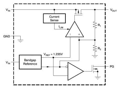
As with other devices in this class, an on-chip comparator in TI TPS797xx devices compares VOUT against an on-chip reference signal (Fig. 1). When VOUT exceeds about 90% of the regulated voltage in TI TPS797xx devices, the power good signal remains asserted until VOUT falls below about 90%.
The Fairchild FAN2558 power good signal provides somewhat tighter tolerance, asserting when the voltage at VOUT is greater than 95% of the specified output voltage – as well as adding additional monitoring conditions including thermal shutdown and overcurrent dropout detection. The Fairchild device also includes a delay in power good output, allowing additional time for power circuits to settle before enabling any load that relies on changes in the power good output signal (Fig. 2).
As with the Fairchild device, the Micrel MIC5248 and MIC5258 LDO ICs also provide a delayed power good signal based on voltage, thermal shutdown, and overcurrent dropout conditions. The Micrel devices offer even tighter tolerance, providing a low threshold that is 89% of Vout and a high threshold 97% of VOUT.
For the power good output signal in its ADP2140 LDO, Analog Devices introduces a small amount of hysteresis in the voltage monitoring circuit, further deglitching the measured signal to reduce the chance that noise or external perturbations might inadvertently trigger the power good signal.
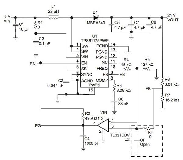
If specifications require a regulator without a power good output, engineers can often design one using available output pins. For example, the Texas Instruments TPS61175 does not provide a built-in power good signal, but engineers can design one using an external comparator such as the Texas Instruments TL331 to compare VOUT with the TPS61175's internal reference, which is tracked by the TPS61175's FREQ output signal (Fig. 3).
Devices designed for energy harvesting applications typically include a built-in power good signal. For example, the Linear Technology LTC3108 and LTC3109 DC/DC converters combine multiple output sources with a power good signal tied to the primary voltage output. Both devices feature a power good threshold of -7.5%, relative to VOUT for rising levels and -9% of Vout for falling levels. The Linear parts feature an additional capability to turn on an auxiliary output supply VOUT2 on these devices. So, for example, the LTC3108/9 power good signal can be used as a power-on reset signal to start an MCU. In turn, the MCU can, as needed, turn on VOUT2 to power external circuits such as sensors and amplifiers that lack their own built-in sleep modes.
Designed with battery management features, the Texas Instruments bq25504 features a similar power good signal with its VBAT_OK output signal. With this device, VBAT_OK is intended to signal an attached MCU when the voltage on an energy storage battery or capacitor has dropped below a pre-set critical level, indicating that loads should be reduced immediately to prevent an undervoltage state from arising. TI recommends that in a practical design, VBAT_OK would be used to drive an external switch placed between its VSTOR voltage output and the load to decouple the load from the energy storage device in an energy harvesting application.
The use of an accurate power good signal is essential in energy harvesting designs driven by varying ambient energy sources. Engineers can take advantage of built-in power good signals in many devices or design a simple power good circuit using external comparators to monitor VOUT against reference voltage levels. In many cases, devices designed specifically for energy harvesting combine power good output signals with multiple voltage sources to provide the flexible power management capabilities required for optimizing power utilization in low power designs.
For energy harvesting designs, the need to rely on trickles of power from ambient energy sources drives a corresponding need not only for careful attention to individual device power consumption and overall power budget, but also the ability to detect when power reaches minimum levels required for circuit operation. For many energy harvesting applications, proper circuit operation entails only recognition that system power has reached the required level. For associated ICs, this recognition comes in the form of a “power good” signal that remains enabled when voltage levels have reached a threshold value set by the engineer.
For more complex designs, engineers can take advantage of sophisticated power management capabilities in dedicated PMICs or specialized energy harvesting devices. For designs intended to minimize device count and system complexity, however, engineers will also discover this functionality built into components typically found at the heart of energy harvesting designs.
Low-dropout (LDO) regulators such as the Texas Instruments TPS797xx family, Fairchild Semiconductor FAN2558, Micrel MIC5248 and MIC5258, and Analog Devices ADP2140, among others, provide a specific “power good” output signal as an open-drain output. Typically used in MCU-based low-power applications, the power good signal provided with this class of device can often be used directly or with just a simple pull-up resistor. It can directly serve as a power-on reset signal for MCUs or low power signal for more general applications.
As with other devices in this class, an on-chip comparator in TI TPS797xx devices compares VOUT against an on-chip reference signal (Fig. 1). When VOUT exceeds about 90% of the regulated voltage in TI TPS797xx devices, the power good signal remains asserted until VOUT falls below about 90%.

Figure 1: In the TI TPS797xx LDO family, the power good signal is asserted when VOUT exceeds about 90% of a reference voltage level as measured by an on-chip comparator (Courtesy of Texas Instruments).
The Fairchild FAN2558 power good signal provides somewhat tighter tolerance, asserting when the voltage at VOUT is greater than 95% of the specified output voltage – as well as adding additional monitoring conditions including thermal shutdown and overcurrent dropout detection. The Fairchild device also includes a delay in power good output, allowing additional time for power circuits to settle before enabling any load that relies on changes in the power good output signal (Fig. 2).

As with the Fairchild device, the Micrel MIC5248 and MIC5258 LDO ICs also provide a delayed power good signal based on voltage, thermal shutdown, and overcurrent dropout conditions. The Micrel devices offer even tighter tolerance, providing a low threshold that is 89% of Vout and a high threshold 97% of VOUT.
For the power good output signal in its ADP2140 LDO, Analog Devices introduces a small amount of hysteresis in the voltage monitoring circuit, further deglitching the measured signal to reduce the chance that noise or external perturbations might inadvertently trigger the power good signal.
If specifications require a regulator without a power good output, engineers can often design one using available output pins. For example, the Texas Instruments TPS61175 does not provide a built-in power good signal, but engineers can design one using an external comparator such as the Texas Instruments TL331 to compare VOUT with the TPS61175's internal reference, which is tracked by the TPS61175's FREQ output signal (Fig. 3).

Devices designed for energy harvesting applications typically include a built-in power good signal. For example, the Linear Technology LTC3108 and LTC3109 DC/DC converters combine multiple output sources with a power good signal tied to the primary voltage output. Both devices feature a power good threshold of -7.5%, relative to VOUT for rising levels and -9% of Vout for falling levels. The Linear parts feature an additional capability to turn on an auxiliary output supply VOUT2 on these devices. So, for example, the LTC3108/9 power good signal can be used as a power-on reset signal to start an MCU. In turn, the MCU can, as needed, turn on VOUT2 to power external circuits such as sensors and amplifiers that lack their own built-in sleep modes.
Designed with battery management features, the Texas Instruments bq25504 features a similar power good signal with its VBAT_OK output signal. With this device, VBAT_OK is intended to signal an attached MCU when the voltage on an energy storage battery or capacitor has dropped below a pre-set critical level, indicating that loads should be reduced immediately to prevent an undervoltage state from arising. TI recommends that in a practical design, VBAT_OK would be used to drive an external switch placed between its VSTOR voltage output and the load to decouple the load from the energy storage device in an energy harvesting application.
The use of an accurate power good signal is essential in energy harvesting designs driven by varying ambient energy sources. Engineers can take advantage of built-in power good signals in many devices or design a simple power good circuit using external comparators to monitor VOUT against reference voltage levels. In many cases, devices designed specifically for energy harvesting combine power good output signals with multiple voltage sources to provide the flexible power management capabilities required for optimizing power utilization in low power designs.
免责声明:各个作者和/或论坛参与者在本网站发表的观点、看法和意见不代表 DigiKey 的观点、看法和意见,也不代表 DigiKey 官方政策。


