Using Cold-Start Circuits to Enable Microwatt Energy Harvesting
投稿人:电子产品
2016-05-10
Energy harvesting can offer power sufficient to eliminate the need for batteries while ensuring continuous operation for years or even decades. For wearable and Internet of Things (IoT) applications, however, available ambient sources may yield converted voltage levels that fall below circuit threshold values. For these designs, engineers can apply methods used to cold-start low-power DC/DC converters or even find power-management ICs (PMICs) with integrated cold-start functionality. Using these low-voltage start-up methods and devices, engineers can ensure device operation even with weak sources of ambient energy.
Harvesting energy from ambient sources offers an effective solution for applications requiring long-term operation without the costs and complications of battery replacement. Ambient energy is often plentiful in industrial applications characterized by high heat and vibration, but in many others, energy harvesting might only yield trickles of power from available energy sources (Table 1.).
| Energy Source | Harvested Power |
|---|---|
| Vibration/Motion | |
| Human | 4 μW/cm2 |
| Industry | 100 μW/cm2 |
| Temperature Difference | |
| Human | 25 μW/cm2 |
| Industry | 1-10 mW/cm2 |
| Light | |
| Indoor | 10 μW/cm2 |
| Outdoor | 10 mW/cm2 |
| RF | |
| GSM | 0.1 μW/cm2 |
| Wi-Fi | 0.001 μW/cm2 |
Table 1: Available ambient sources might offer very low power, particularly for wearables and IoT devices that rely on human-powered energy extraction or low-power Wi-Fi energy harvesting. (Courtesy of Texas Instruments)
Although semiconductor process technologies continue to reduce device threshold voltages, even the most efficient energy-harvesting methods may only generate subthreshold voltage levels.
Start-up circuits
With a typical high-efficiency DC/DC converter, very-low-voltage inputs are insufficient to energize the internal voltage-conversion circuitry. In fact, DC/DC converter specifications include a minimum input voltage level required for operation. Cold-start circuits serve to bootstrap conversion circuits when voltage levels fall below minimum levels. In these circuits, low-input-voltage levels are sufficient to drive an oscillator that, in turn, drives the switches of a start-up switched-boost converter that sacrifices efficiency for the ability to operate at low voltage levels. As input voltage rises, the energy-harvesting system can disable the start-up converter and allow operations to proceed with a more efficient converter.
Energy-harvesting designers can find PMICs with low-voltage cold-start functionality that implement this kind of start-up oscillator circuit and use its output to drive the gates in a switched-boost converter. For example, Texas Instruments uses a start-up oscillator in its TPS61220 converter (Figure 1). If the input voltage to this device is not high enough to supply its control circuit properly, a start-up oscillator operates the switches integrated into the device. During this phase, the oscillator controls the switching frequency, and the maximum switch current is limited. When the device has built up the output voltage high enough to supply the control circuit (approximately 1.8 V), the device switches to its normal operating mode.

Figure 1: In the Texas Instruments TPS61220 series, a start-up oscillator drives a pair of MOSFET gates when Vin remains at subthreshold voltage levels (A); an inductor on L pin and output capacitor across Vout to ground complete the familiar switching-boost topology (B). (Courtesy of Texas Instruments)
Bootstrap sequence
Although these bootstrap converters offer limited power output, their output can be sufficient to drive more efficient switching regulators designed to take over the conversion process and disable the low-efficiency start-up converter. STMicroelectronics uses this approach in its SPV1050, which integrates both a low-voltage charge-pump boost converter and a high-efficiency buck-boost switching converter.
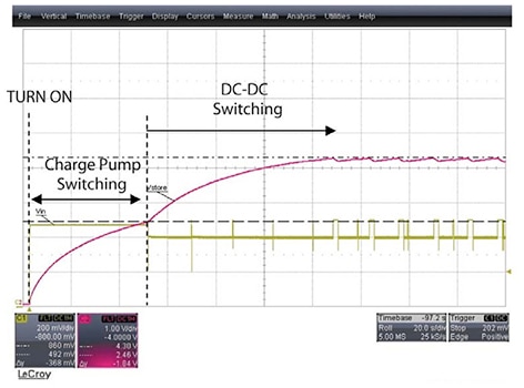
When the energy transducer is connected, the SPV1050 device (Figure 2) will start with input voltages as low as 120 mV. While levels remain below 2.6 V, the device uses its integrated high-efficiency charge pump to boost the voltage, and the switched converter remains disabled. Above 2.6 V, voltage is boosted by the device’s integrated switching converter.

Figure 2: In the STMicroelectronics SPV1050 energy-harvesting device, an integrated charge pump provides an initial boost to raise harvested voltage to levels sufficient for operation of a more efficient switching converter that is also integrated in the device. (Courtesy of STMicroelectronics)
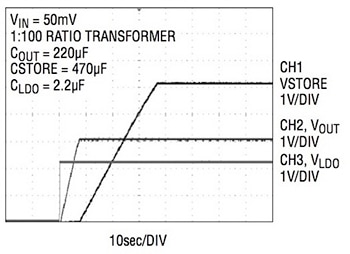
Designers can achieve even lower cold-start voltage levels by using start-up circuits that incorporate a transformer with a high primary-to-secondary turns ratio. Linear Technology uses this approach in its LTC3108, which uses an external transformer, small coupling capacitor, and MOSFET switch to form a resonant oscillator. The transformer’s turns ratio determines the minimum input voltage required for start-up. With the LTC3108, the use of a transformer with a 1:100 ratio allows the device to achieve start-up voltages as low as 20 mV. In practice, the characteristics of each specific application will affect performance and as the DC resistance of the transformer windings rises, the efficiency of conversion will fall.
While start-up circuitry is responsible for energizing low-voltage boost converters, additional circuitry is typically needed to complete the start-up process for more complex devices. Linear’s LTC3108 offers multiple output voltage sources including a precision voltage reference, low dropout (LDO) regulator, and programmable output-voltage levels. After the boosted voltage passes through LTC3108’s internal rectifiers during the start-up phase, this rectified voltage (VAUX) supplies the device’s internal circuit.
During the start-up process, as VAUX rises, different internal circuits are activated in a carefully controlled sequence (Figure 3). When VAUX exceeds 2 V, the device’s precision reference becomes active. In addition, synchronous rectifiers in parallel with each of the internal diodes take over input-voltage rectification from those internal diodes to achieve improved efficiency. At 2.2 V, the device’s integrated LDO becomes active, and when Vaux exceeds 2.5 V, the main Vout output is allowed to start charging.

Figure 3: Linear Technology’s LTC3108 energy-harvesting IC combines a cold-start functionality with power sequencing features able to ensure proper voltage levels at each of the device’s outputs. (Courtesy of Linear Technology)
Summary
Energy harvesting offers a virtually inexhaustible source of power able to support battery-free operation of low-power design for years or decades. For many wearable and IoT designs, however, available ambient sources might present weak energy sources, at times offering voltage levels well below the operating minimums of typical voltage converters. In these applications, start-up circuits boost very low-level voltage inputs, using a combination of self-starting oscillators and simple boost converters. These start-up circuits typically achieve low-voltage operation at the cost of conversion efficiency. Consequently, more efficient energy-harvesting designs combine these low-efficiency start-up circuits with high-efficiency switching converters able to take over conversion as voltage levels rise.
For more information about the parts discussed in this article, use the links provided to access product pages on the DigiKey website.
免责声明:各个作者和/或论坛参与者在本网站发表的观点、看法和意见不代表 DigiKey 的观点、看法和意见,也不代表 DigiKey 官方政策。


