Use IO-Link Transceivers to Cut Power, Boost Performance, and Simplify Development
投稿人:DigiKey 北美编辑
2017-11-02
IO-Link is proving popular for connecting sensors, actuators, and systems in industrial environments. Still, developers face a growing list of demands for more capabilities, higher performance, and lower power dissipation, for both master and device transceivers.
Using a pair of devices from Maxim Integrated, engineers can meet these needs, and rapidly implement robust IO-Link connectivity.
This article will examine the requirements of industrial sensor networks, the issues designers face, and how IO-Link meets the requirements of these networks. It will then introduce IO-Link solutions from Maxim Integrated, and show how they can be used to rapidly implement fully compliant IO-Link connectivity between network-gateway systems and large numbers of peripheral sensors and actuators.
IO-Link enables massive sensor deployments
Advanced industrial systems lean heavily on engineers’ abilities to deploy hundreds or even thousands of sensors and actuators in harsh manufacturing environments. In moving to smart MCU-based devices, engineers not only must maintain connectivity with older legacy devices and systems, but address growing challenges in reducing power despite continued growth in the size and complexity of devices and systems. IO-Link has earned a vital role in these environments with its ability to maintain backward compatibility while supporting increasingly sophisticated sensors and actuators connected through different industrial networks. By providing a standard input/output (I/O) connectivity technology, IO-Link enables engineers to easily combine diverse peripherals and systems.
Standard I/O interface
On the factory floor, IO-Link defines a standard interface for connecting factory systems to peripheral devices including sensors and actuators. IO-Link maintains the 24 volt supply and signal heritage of legacy peripherals, using its three-wire interface to provide 24 volt power on two lines (L+ and L-), along with serial communications on the third wire (C/Q). In processor-based systems, IO-Link compatible transceivers lay on either end of an IO-Link connection. They communicate with each other using IO-Link physical protocols. At the same time, they are converting the IO-Link signaling levels to conventional digital levels for MCUs and processors connected to the transceivers through a UART or SPI bus (Figure 1).
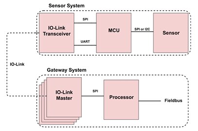
Figure 1: IO-Link defines a point-to-point connection interface between sensor or actuator systems on the factory floor and gateway systems connecting those peripheral devices to factory networks. (Image created using DigiKey Scheme-it®)
While IO-Link transceivers support the lower, physical layers of the IO-Link specification, the attached MCU or processor typically manages IO-Link’s higher-level functional capabilities using a simple messaging protocol. Each IO-Link transaction occurs in a message sequence (M-sequence), which starts with a command message from the master, and ends with a response message from the connected device. Within the M-sequence, both master and device messages comprise a short series of UART frames containing data or byte commands defined by the IO-Link specification, and are delivered with timing dependent on the device, master, and application (Figure 2).

Figure 2: IO-Link specifies a simple messaging sequence (M-sequence), where a master transmits a command as a series of UART frames to a peripheral device and receives response from the device. (Image source: Maxim Integrated)
IO-Link defines a variety of capabilities designed to ensure reliable communications in harsh environments. It allows transceivers to retry transmitting frames with eventual defined failure modes on continued unsuccessful attempts. IO-Link also specifies methods for peripheral devices to store information about themselves in standard I/O device description (IODD) blocks, and provide that information on command from an IO-Link master. An IO-Link master can use this device configuration information to set cycle times and data rates, while still falling back to slower speeds, if required, to maintain reliable communications.
While IO-Link offers broad advantages and features beyond the scope of this article, industrial automation developers are demanding more of it. At the most fundamental level, the continued growth in number and capabilities of sensors and other peripheral devices imposes significant demand on both ends of an IO-Link connection. IO-Link masters need more sophisticated capabilities for delivering L+ power efficiently and safely to more advanced peripheral devices.
On the periphery, IO-Link transceivers face requirements for simplified design in MCU-based systems. For both master and device transceiver, developers need to minimize power consumption to reduce thermal load as more advanced gateway systems move to fanless designs to reduce power, eliminate noise, and simplify maintenance on the factory floor. A pair of devices from Maxim Integrated address these expanding requirements with simple, low-power solutions for implementing IO-Link interfaces.
Efficient gateways
The Maxim Integrated MAX14819 master transceiver offers a single-chip solution for creating IO-Link gateway systems. Designed to simplify IO-Link interface design, the device fully supports two IO-Link channels through separate L+ supply controllers and frame handlers dedicated to each channel. For all its extensive functionality, the device typically consumes only 1.9 milliamps (mA), and even less if developers use an external step-down regulator such as the Maxim Integrated MAX15062A instead of the MAX14819 transceiver’s internal 5 volt regulator. Thanks to the device’s integrated functionality, developers need only connect the MAX14819 to an MCU through SPI and UART interfaces, and add a few components to provide a fully compliant, low-power IO-Link gateway (Figure 3).
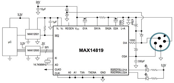
Figure 3: Developers can implement an IO-Link master using an MCU, the Maxim Integrated MAX14819, and only a few additional components. (Image source: Maxim Integrated)
Though the component count is minimal, it’s wise to add isolators, such as Maxim Integrated’s MAX12930 Opto isolators and MAX12931 digital isolators.
As mentioned, the IO-Link standard specifies L+/L- supply lines, also called sensor supply. These are provided through cables that can run up to 20 meters (m) and are not required to be shielded according to the standard. To ensure safety and reliability in harsh environments, the MAX14819 sensor supply controllers provide settable current limiting, reverse current blocking, and reverse polarity protection capability.
Connecting G1x to the gate of a low-RDS(ON) MOSFET such as the ON Semiconductor NTTFS5116PL, the device can control external reverse current blocking for the sensor supply for the corresponding channel without adding significant thermal load. A similar MOSFET at G2x drives current to the corresponding A or B sensor supply channel. A sensor resistor placed between SN1x and SN2x sets the current limit for that sensor supply channel. Beyond these basic protection capabilities, the MAX14819 lets developers set the device’s configuration registers to set optimization parameters such as turn-on time, current-limiting blanking time, and autoretry delay for each sensor supply.
To help ensure signal integrity on the CQx line, the MAX14819 combines automatic protection features with settable features that developers can program using the device’s configuration registers. For example, using configuration registers, the designer can set CQx current limiting to different values, ranging from 100 mA to 500 mA, as well as set blanking time. If an overcurrent condition lasts longer than the blanking time, the device can generate an interrupt and enter retry mode, depending on the register settings.
In gateway designs, however, the requirements for IO-Link master devices extend beyond those required to support IO-Link supply and signaling requirements for individual sensors. In supporting the need for more IO-Link channels, host processors can be overwhelmed when executing the data-link layer operations required to meet IO-Link requirements. Instead, designers can use the MAX14819’s integrated frame handler to mitigate this condition.
Frame handler
The MAX14819 complements its support for sensor supply and CQ protection on the peripheral side with integrated frame handlers that offload the host processor, providing time-critical control of IO-Link M-sequences. Operating independently, the MAX14819 enables developers to achieve IO-Link cycle times as fast as 400 microseconds (µs), all with minimal impact on the host processor.
Frame handling plays a fundamental role in the IO-Link messaging protocol. To perform a typical M-sequence transaction, the designer loads a master message from the host processor into a MAX14819 FIFO buffer through the shared SPI bus, either in a burst or as a series of byte writes. The MAX14819 transmits the message in a corresponding series of frames through CQx and immediately switches the CQx channel to receive mode, awaiting the device response message. On receipt, the MAX14819 loads the device message into a receive buffer and toggles RXRDYBx, which can also serve as an interrupt to notify the host (Figure 4). In turn, the host uses the SPI bus to read the receive buffer, which automatically resets the RXRDYBx line.
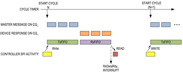
Figure 4: The Maxim Integrated MAX14819’s integrated frame handler simplifies IO-Link transactions, requiring only a SPI write to the MAX14819 to start an IO-Link cycle and a SPI read to access the result when a data-ready interrupt occurs. (Image source: Maxim Integrated)
In an IO-Link system, the master determines the minimum cycle time automatically by reading the IODD during the startup sequence (or overriding these values to meet application-specific cycle time requirements). Within a cycle, engineers can configure the MAX14819 to generate a fault if the device message is not received within the expected tM-sequence time period – a requirement of the IO-Link specification. In practice, however, IO-Link devices may require more time than the IO-Link standard tM-sequence time period, which the standard defines as a function of the length of the master and device messages and the interframe intervals (see Figure 2 again).
The MAX14819 allows developers to adjust the allowed delay before the device generates an RxERR interrupt that signifies a receive error. Although this approach departs from the strict definition of the IO-Link standard, it addresses a problem sometimes encountered in real-world environments.
Along with its flexibility in addressing real-world implementation problems, the MAX14819 supports a variety of system design approaches. As illustrated earlier (see Figure 3, again), developers can rely on the MAX14819’s integrated functionality to rapidly implement an IO-Link master design.
However, if necessary, developers can use the MAX14819 simply as an IO-Link transceiver, connecting the MAX14819’s TXENx, TXx, and RXx pins to the corresponding UART ports of the processor. In this mode, all communication moves through the UART ports, bypassing the MAX14819’s frame handler, moving through buffers directly to its CQx (A and B) ports (Figure 5).
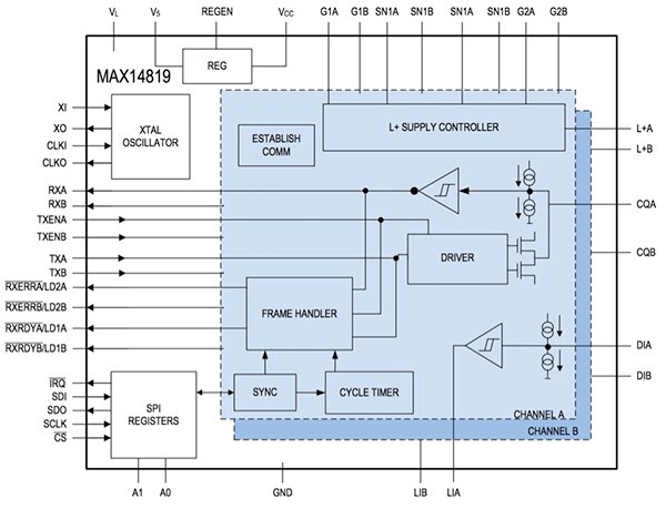
Figure 5: The Maxim Integrated MAX14819 extends the conventional IO-Link transceiver functionality with integrated L+ supply controllers and frame handlers able to offload data-link processing from the host processor. (Image source: Maxim Integrated)
For typical IO-Link gateway designs, however, designers are more likely to take advantage of the MAX14819’s complete IO-Link functionality. To meet growing requirements for more channels, designers will typically combine multiple masters in a single system. The MAX14819 provides a pair of SPI chip address pins, allowing designers to combine four MAX14819 devices on the same SPI bus. Each device monitors the SPI address included in any read/write cycle and responds to commands with matching addresses.
Although developers can implement an IO-Link master relatively easily with a MAX14819, an MCU, and a few additional components, the detailed design of a full gateway system can add delays in implementation. For example, real-world gateway systems face inductive loads that require external transient voltage protection and clamping diodes to absorb energy.
To help developers create these systems more rapidly, Maxim Integrated offers its MAXREFDES145 eight-channel IO-Link gateway reference design (Figure 6). Along with the board, the reference design includes full schematics and BOM, providing developers with an immediate design solution or the foundation of a custom implementation.
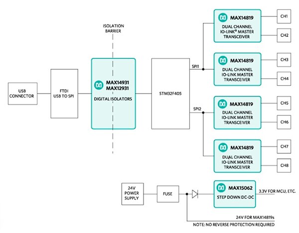
Figure 6: The Maxim Integrated MAXREFDES145 reference design demonstrates a complete IO-Link-compliant gateway design that uses a single STMicroelectronics STM32F405RGT6 MCU to manage multiple IO-Link master channels. (Image source: Maxim Integrated)
Sensor systems
While IO-Link master devices face requirements for multiple connections, L+ supply control, and frame handling, sensors and actuators at the device end of an IO-Link connection bring additional requirements for IO drive capability, different regulated voltage supplies, and sensor interface protection. At the same time, MCUs used in these peripheral devices typically provide more than enough processing power to handle IO-Link data-link layer operations for its single connection to the gateway. For these sensor/actuator designs, the Maxim Integrated MAX14827A transceiver provides an effective solution, providing similar line protection features as the MAX14819 while addressing the unique requirements of peripheral systems.
In an IO-Link-compatible design, the MAX14827A works as a companion device with the MCU used in a typical peripheral device design (see Figure 1, again). Here, the designer connects the MAX14827A to the MCU’s UART ports in the same way described earlier for use of the MAX14819 in transceiver-only mode. The transceiver supports the IO-Link low-level physical interface requirements, transmitting and receiving UART frames in M-sequences managed by the MCU.
In a typical design, engineers would configure and monitor the MAX14827A by accessing the device’s registers through the device’s SPI ports, while using the UART interface to send and receive IO-Link frames. For simple MCUs that do not provide separate SPI and UART ports, this parallel operating mode would be unavailable. For these cases, the MAX14827A provides alternative approaches. In multiplexed mode, the MAX14827A SPI and UART ports can share a single serial port on the MCU, taking advantage of idle periods in the IO-Link cycle to multiplex SPI and UART communications on the single channel. The MAX14827A’s pin mode offers an even simpler operating mode, controlling device operation by managing levels on the device’s pins.
Along with addressing alternative MCU-based design features, the MAX14827A helps simplify peripheral system design through its integrated voltage regulators. Instead of adding external voltage regulators to power sensors, conditioning circuits, and other circuits, designers can tie into the regulated 3.3 volt and 5 volt supply rails provided by the device. Of course, engineers can bypass these on-chip sources in favor of external regulators.
As with the MAX14819 master device, the MAX14827A transceiver requires few additional components to add basic IO-Link functionality to an existing MCU-based sensor or actuator design. Nevertheless, designers would typically augment the base MAX14827A circuit with additional circuits such as those for transient voltage protection (Figure 7). To help speed development, Maxim Integrated provides the MAX14827EVKIT evaluation board, which provides a complete IO-Link transceiver implementation that addresses practical design considerations such as TVS protection.
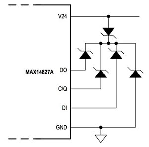
Figure 7: Although the Maxim Integrated MAX14827A provides built-in protection features, developers would typically add more protection. (Image source: Maxim Integrated)
To be on the safe side, designers should add transient voltage protection to the DO, C/Q, and DI lines, using transient voltage suppression (TVS) diodes such as the STMicroelectronics SMAJ33A.
Conclusion
IO-Link offers a standard, robust protocol for interconnecting sensors and actuators with factory networks. Yet, practical concerns over power consumption, thermal management, design size, and performance loom as significant challenges for engineers looking to develop IO-Link compliant systems. Using the Maxim Integrated MAX14819 master transceiver and MAX14827A device transceiver, engineers can rapidly implement fully compliant IO-Link connectivity between network-gateway systems and large numbers of peripheral sensors and actuators.

免责声明:各个作者和/或论坛参与者在本网站发表的观点、看法和意见不代表 DigiKey 的观点、看法和意见,也不代表 DigiKey 官方政策。





 中国
中国